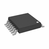
AD5280BRUZ200 Analog Devices Inc, AD5280BRUZ200 Datasheet - Page 4

AD5280BRUZ200
Manufacturer Part Number
AD5280BRUZ200
Description
IC,Digital Potentiometer,TSSOP,14PIN,PLASTIC
Manufacturer
Analog Devices Inc
Datasheet
1.AD5280BRUZ50.pdf
(28 pages)
Specifications of AD5280BRUZ200
Taps
256
Resistance (ohms)
200K
Number Of Circuits
1
Temperature Coefficient
30 ppm/°C Typical
Memory Type
Volatile
Interface
I²C, 2-Wire Serial
Voltage - Supply
4.5 V ~ 16.5 V, ±4.5 V ~ 5.5 V
Operating Temperature
-40°C ~ 85°C
Mounting Type
Surface Mount
Package / Case
14-TSSOP
Resistance In Ohms
200K
Lead Free Status / RoHS Status
Lead free / RoHS Compliant
AD5280/AD5282
Parameter
INTERFACE TIMING CHARACTERISTICS (applies to all parts)
1
2
3
4
5
6
7
8
9
10
11
Typicals represent average readings at 25°C, V
Resistor position nonlinearity error R-INL is the deviation from an ideal value measured between the maximum resistance and the minimum resistance wiper
positions. R-DNL measures the relative step change from ideal between successive tap positions. Parts are guaranteed monotonic.
V
INL and DNL are measured at V
of ±1 LSB maximum are guaranteed monotonic operating conditions.
Resistor Terminal A, Resistor Terminal B, and Wiper Terminal W have no limitations on polarity with respect to each other.
Guaranteed by design and not subject to production test.
P
Bandwidth, noise, and settling time are dependent on the terminal resistance value chosen. The lowest R value results in the fastest settling time and highest
bandwidth. The highest R value results in the minimum overall power consumption.
All dynamic characteristics use V
See timing diagram (Figure 3) for location of measured values.
Standard I
AB
DISS
Total Harmonic Distortion
V
Crosstalk
Analog Crosstalk
Resistor Noise Voltage
SCL Clock Frequency
t
t
t
t
t
t
t
t
t
t
BUF
HD:STA
LOW
HIGH
SU:STA
HD:DAT
SU:DAT
F
R
SU:STO
W
= V
Fall Time of Both SDA and
Rise Time of Both SDA and
is calculated from (I
Stop and Start
Start)
Condition
SCL Signals
SCL Signals
Condition
Settling Time
Bus Free Time Between
Low Period of SCL Clock
DD
High Period of SCL Clock
SDA
SCL
Setup Time for Start
Hold Time (Repeated
Data Setup Time
Setup Time for STOP
Data Hold Time
, wiper (V
2
C mode operation is guaranteed by design.
W
) = no connect.
P
DD
t
1
× V
S
DD
W
). CMOS logic level inputs result in minimum power dissipation.
DD
with the RDAC configured as a potentiometer divider similar to a voltage output DAC. V
= 5 V.
t
2
Symbol
THD
t
CT
CTA
e
f
t
t
t
t
t
t
t
t
t
t
SCL
S
1
2
3
4
5
6
7
8
9
10
N_WB
t
DD
3
W
= +5 V, V
t
8
t
8
SS
= −5 V.
t
9
Figure 3. Detailed Timing Diagram
t
6
6, 10, 11
Conditions
V
V
V
V
adjacent RDAC making full-scale
code change
Measure V
10 kHz
R
After this period, the first clock pulse
is generated
A
B
A
A
WB
= 0 V dc, f = 1 kHz
= 1 V rms, R
= 5 V, V
= V
t
Rev. C | Page 4 of 28
= 20 kΩ, f = 1 kHz
t
4
9
DD
, V
B
B
W1
= 5 V, ±1 LSB error band
= 0 V, measure V
with V
AB
= 20 kΩ
t
7
W2
= 5 V p-p @ f =
W1
S
with
t
5
t
2
Min
0
1.3
0.6
1.3
0.6
0.6
0
100
0.6
A
= V
DD
and V
Typ
0.014
5
15
−62
18
B
= 0 V. DNL specification limits
1
Max
400
0.9
300
300
P
t
10
Unit
%
μs
nV-s
dB
nV/√Hz
kHz
μs
μs
μs
μs
μs
μs
ns
ns
ns
μs


