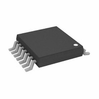
AD5280BRUZ200 Analog Devices Inc, AD5280BRUZ200 Datasheet - Page 18

AD5280BRUZ200
Manufacturer Part Number
AD5280BRUZ200
Description
IC,Digital Potentiometer,TSSOP,14PIN,PLASTIC
Manufacturer
Analog Devices Inc
Datasheet
1.AD5280BRUZ50.pdf
(28 pages)
Specifications of AD5280BRUZ200
Taps
256
Resistance (ohms)
200K
Number Of Circuits
1
Temperature Coefficient
30 ppm/°C Typical
Memory Type
Volatile
Interface
I²C, 2-Wire Serial
Voltage - Supply
4.5 V ~ 16.5 V, ±4.5 V ~ 5.5 V
Operating Temperature
-40°C ~ 85°C
Mounting Type
Surface Mount
Package / Case
14-TSSOP
Resistance In Ohms
200K
Lead Free Status / RoHS Status
Lead free / RoHS Compliant
AD5280/AD5282
LEVEL SHIFT FOR BIDIRECTIONAL INTERFACE
While most old systems can be operated at one voltage, a new
component can be optimized at another. When two systems
operate the same signal at two different voltages, proper level
shifting is needed. For instance, a 3.3 V EEPROM can interface
with a 5 V digital potentiometer. A level-shift scheme is needed
to enable a bidirectional communication so that the setting of
the digital potentiometer can be stored to and retrieved from
the EEPROM. Figure 49 shows one of the implementations.
M1 and M2 can be any N-channel signal FETs or low threshold
FDV301N if V
LEVEL SHIFT FOR NEGATIVE VOLTAGE
OPERATION
The digital potentiometer is popular in laser diode driver
applications and certain telecommunications equipment level-
setting applications. These applications are sometimes
operated between ground and a negative supply voltage such
that the systems can be biased at ground to avoid large bypass
capacitors that may significantly impede the ac performance.
Like most digital potentiometers, the AD5280/AD5282 can be
configured with a negative supply (see Figure 50).
However, the digital inputs must also be level shifted to allow
proper operation because the ground is referenced to the
negative potential. Figure 51 shows one implementation with a
few transistors and a few resistors. When V
threshold value, Q3 is off, Q1 is off, and Q2 is on. In this state,
V
and Q2 is turned off. In this state, V
Be aware that proper time shifting is also needed for successful
communication with the device.
OUT
V
SDA1
SCL1
DD1
approaches 0 V. When V
= 3.3V
Figure 49. Level Shift for Different Potential Operation
EEPROM
3.3V
DD
LEVEL SHIFTED
LEVEL SHIFTED
R
P
Figure 50. Biased at Negative Voltage
falls below 2.5 V.
R
P
S
M1
–5V
G
D
IN
S
is above 2 V, Q3 is on, Q1 is on,
M2
G
V
V
GND
SDA
SCL
DD
SS
OUT
D
is pulled down to V
R
IN
P
is below the Q3
AD5282
R
P
5V
V
DD2
SDA2
SCL2
= 5V
SS
Rev. C | Page 18 of 28
.
ESD PROTECTION
All digital inputs are protected with a series input resistor and
parallel Zener ESD structures, as shown in Figure 52. The
protection applies to digital inputs SDA, SCL, and SHDN .
TERMINAL VOLTAGE OPERATING RANGE
The AD5280/AD5282 positive V
supply defines the boundary conditions for proper 3-terminal
digital potentiometer operation. Supply signals present on
Resistor Terminal A, Resistor Terminal B, and Wiper Terminal
W that exceed V
biased diodes (see Figure 53).
POWER-UP SEQUENCE
Because there are ESD protection diodes that limit the voltage
compliance at Terminal A, Terminal B, and Terminal W (see
Figure 53), it is important to power V
voltage to the A, B, and W terminals. Otherwise, the diode is
forward biased such that V
which may affect the rest of the user’s circuit. The ideal power-
up sequence is the following: GND, V
V
is not important as long as they are powered after V
A
/V
B
/V
Figure 53. Maximum Terminal Voltages Set by V
+5V
W
0
. The order of powering V
Figure 51. Level Shift for Bipolar Potential Operation
Figure 52. ESD Protection of Digital Pins
DD
V
IN
or V
0
340Ω
V
SS
SS
V
are clamped by the internal forward-
= –5V
DD
Q3
Q1
DD
V
R2
10kΩ
SS
/V
SS
LOGIC
DD
is unintentionally powered,
and negative V
A
/V
DD
DD
Q2
/V
V
A
W
B
V
, V
B
R3
10kΩ
/V
DD
SS
SS
SS
0
W
–5V
before applying any
, digital inputs, and
and digital inputs
0
V
OUT
DD
and V
SS
DD
power
/V
SS
SS
.


