AD5280BRUZ200 Analog Devices Inc, AD5280BRUZ200 Datasheet - Page 6

AD5280BRUZ200
Manufacturer Part Number
AD5280BRUZ200
Description
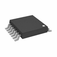
IC,Digital Potentiometer,TSSOP,14PIN,PLASTIC
Manufacturer
Analog Devices Inc
Datasheet
1.AD5280BRUZ50.pdf
(28 pages)
Specifications of AD5280BRUZ200
Taps
256
Resistance (ohms)
200K
Number Of Circuits
1
Temperature Coefficient
30 ppm/°C Typical
Memory Type
Volatile
Interface
I²C, 2-Wire Serial
Voltage - Supply
4.5 V ~ 16.5 V, ±4.5 V ~ 5.5 V
Operating Temperature
-40°C ~ 85°C
Mounting Type
Surface Mount
Package / Case
14-TSSOP
Resistance In Ohms
200K
Lead Free Status / RoHS Status
Lead free / RoHS Compliant
AD5280/AD5282
PIN CONFIGURATIONS AND FUNCTION DESCRIPTIONS
Table 4. AD5280 Pin Function Descriptions
Pin No.
1
2
3
4
5
6
7
8
9
10
11
12
13
14
Mnemonic
A
W
B
V
SHDN
SCL
SDA
AD0
AD1
GND
V
O
V
O
DD
SS
L
2
1
SHDN
Figure 4. AD5280 Pin Configuration
SDA
SCL
V
DD
W
A
B
Description
Resistor Terminal A.
Wiper Terminal W.
Resistor Terminal B.
Positive Power Supply. Specified for
operation from 5 V to 15 V (sum of |V
+ |V
Active Low, Asynchronous Connection
of Wiper W to Terminal B and Open
Circuit of Terminal A. RDAC register
contents unchanged. SHDN should tie
to V
programmable preset in power-up.
Serial Clock Input.
Serial Data Input/Output.
Programmable Address Bit 0 for
Multiple Package Decoding. Bit AD0
and Bit AD1 provide four possible
addresses.
Programmable Address Bit 1 for
Multiple Package Decoding. Bit AD0
and Bit AD1 provide four possible
addresses.
Common Ground.
Negative Power Supply. Specified for
operation from 0 V to −5 V (sum of |V
+ |V
Logic Output Terminal O
Logic Supply Voltage. Needs to be less
than or equal to V
voltage as the digital logic controlling
the AD5280.
Logic Output Terminal O
1
2
3
4
5
6
7
SS
L
SS
AD5280
TOP VIEW
if not used. Can also be used as a
| ≤ 15 V).
| ≤ 15 V).
14
13
12
11
10
9
8
DD
O
V
O
V
GND
AD1
AD0
L
SS
1
2
and at the same
2.
1
.
DD
DD
Rev. C | Page 6 of 28
|
|
Table 5. AD5282 Pin Function Descriptions
Pin No.
1
2
3
4
5
6
7
8
9
10
11
12
13
14
15
16
Mnemonic
O
A
W
B
V
SHDN
SCL
SDA
AD0
AD1
GND
V
V
B
W
A
1
DD
SS
L
2
1
2
1
1
2
SHDN
Figure 5. AD5282 Pin Configuration
SDA
SCL
V
W
O
A
B
DD
1
1
1
1
Description
Logic Output Terminal O
Resistor Terminal A
Wiper Terminal W
Resistor Terminal B
Positive Power Supply. Specified for
operation from 5 V to 15 V (sum of |V
+ |V
Active Low, Asynchronous Connection
of Wiper W to Terminal B and Open
Circuit of Terminal A. RDAC register
contents unchanged. SHDN should tie
to V
programmable preset in power-up.
Serial Clock Input.
Serial Data Input/Output.
Programmable Address Bit 0 for
Multiple Package Decoding. Bit AD0
and Bit AD1 provide four possible
addresses.
Programmable Address Bit 1 for
Multiple Package Decoding. Bit AD0
and Bit AD1 provide four possible
addresses.
Common Ground.
Negative Power Supply. Specified for
operation from 0 V to −5 V (sum of |V
+ |V
Logic Supply Voltage. Needs to be less
than or equal to V
voltage as the digital logic controlling
the AD5282.
Resistor Terminal B
Wiper Terminal W
Resistor Terminal A
1
2
3
4
5
6
7
8
SS
L
SS
AD5282
TOP VIEW
if not used. Can be also used as a
| ≤ 15 V).
| ≤ 15 V).
16
15
14
13
12
11
10
9
1
2
DD
A
W
B
V
V
GND
AD1
AD0
.
.
1
2
1
2
2
2
L
SS
.
.
.
.
2
and at the same
1
.
DD
DD
|
|


