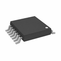
AD5280BRUZ200 Analog Devices Inc, AD5280BRUZ200 Datasheet - Page 16

AD5280BRUZ200
Manufacturer Part Number
AD5280BRUZ200
Description
IC,Digital Potentiometer,TSSOP,14PIN,PLASTIC
Manufacturer
Analog Devices Inc
Datasheet
1.AD5280BRUZ50.pdf
(28 pages)
Specifications of AD5280BRUZ200
Taps
256
Resistance (ohms)
200K
Number Of Circuits
1
Temperature Coefficient
30 ppm/°C Typical
Memory Type
Volatile
Interface
I²C, 2-Wire Serial
Voltage - Supply
4.5 V ~ 16.5 V, ±4.5 V ~ 5.5 V
Operating Temperature
-40°C ~ 85°C
Mounting Type
Surface Mount
Package / Case
14-TSSOP
Resistance In Ohms
200K
Lead Free Status / RoHS Status
Lead free / RoHS Compliant
AD5280/AD5282
DIGITAL INTERFACE
2-WIRE SERIAL BUS
The AD5280/AD5282 are controlled via an I
bus. The RDACs are connected to this bus as slave devices. As
shown in Figure 45, Figure 46, and Table 6, the first byte of the
AD5280/AD5282 is a slave address byte. It has a 7-bit slave
address and an R/ W bit.
The 5 MSBs are 01011, and the two bits that follow are deter-
mined by the state of the AD0 pin and the AD1 pin of the
device. AD0 and AD1 allow the user to place up to four of the
I
protocol operates as follows.
The master initiates data transfer by establishing a start condi-
tion, which happens when a high-to-low transition on the SDA
line occurs while SCL is high (see Figure 45). The following
byte is the slave address byte, which consists of the 7-bit slave
address followed by an R/ W bit (this bit determines whether
data is read from or written to the slave device).
The slave whose address corresponds to the transmitted address
responds by pulling the SDA line low during the ninth clock
pulse (this is called the acknowledge bit). At this stage, all other
devices on the bus remain idle while the selected device waits for
data to be written to or read from its serial register. If the R/ W bit
is high, the master reads from the slave device. On the other
hand, if the R/ W bit is low, the master writes to the slave device.
A write operation contains one instruction byte more than a
read operation. Such an instruction byte in write mode follows
the slave address byte. The most significant bit (MSB) of the
instruction byte labeled A /B is the RDAC subaddress select. A
low selects RDAC1 and a high selects RDAC2 for the dual
channel AD5282. Set A /B low for the AD5280.
RS, the second MSB, is the midscale reset. A logic high on this
bit moves the wiper of a selected channel to the center tap
where RWA = RWB. This feature effectively writes over the
contents of the register and thus, when taken out of reset mode,
the RDAC remains at midscale.
SD, the third MSB, is a shutdown bit. A logic high causes the
selected channel to open circuit at Terminal A while shorting
the wiper to Terminal B. This operation yields almost 0 Ω i n
rheostat mode or 0 V in potentiometer mode. This SD bit serves
the same function as the SHDN pin except that the SHDN pin
reacts to active low. Also, the SHDN pin affects both channels
(AD5282) as opposed to the SD bit, which affects only the
channel that is being written to. Note that the shutdown
2
C-compatible devices on one bus. The 2-wire I
2
C-compatible serial
2
C serial bus
Rev. C | Page 16 of 28
operation does not disturb the contents of the register. When
brought out of shutdown, the previous setting is applied to
the RDAC.
The following two bits are O
mable logic outputs that can be used to drive other digital loads,
logic gates, LED drivers, analog switches, and so on. The three
LSBs are don’t care bits (see Figure 45).
After acknowledging the instruction byte, the last byte in write
mode is the data byte. Data is transmitted over the serial bus in
sequences of nine clock pulses (eight data bits followed by an
acknowledge bit). The transitions on the SDA line must occur
during the low period of SCL and remain stable during the high
period of SCL (see Figure 45).
In read mode, the data byte follows immediately after the
acknowledgment of the slave address byte. Data is transmitted
over the serial bus in sequences of nine clock pulses (a slight
difference from write mode, where there are eight data bits
followed by an acknowledge bit). Similarly, the transitions on
the SDA line must occur during the low period of SCL and
remain stable during the high period of SCL (see Figure 46).
When all data bits have been read or written, a stop condition is
established by the master. A stop condition is defined as a low-
to-high transition on the SDA line while SCL is high. In write
mode, the master pulls the SDA line high during the tenth clock
pulse to establish a stop condition (see Figure 45). In read
mode, the master issues a no acknowledge for the ninth clock
pulse (that is, the SDA line remains high). The master then
brings the SDA line low before the 10th clock pulse, which goes
high to establish a stop condition (see Figure 46).
A repeated write function gives the user flexibility to update the
RDAC output a number of times after addressing and instructing
the part only once. During the write cycle, each data byte updates
the RDAC output. For example, after the RDAC has acknow-
ledged its slave address and instruction bytes, the RDAC output
updates after these two bytes. If another byte is written to the
RDAC while it is still addressed to a specific slave device with the
same instruction, this byte updates the output of the selected slave
device. If different instructions are needed, the write mode has to
start with a new slave address, instruction, and data byte again.
Similarly, a repeated read function of RDAC is also allowed.
1
and O
2
. They are extra program-


