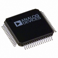
AD7606BSTZ-6RL Analog Devices Inc, AD7606BSTZ-6RL Datasheet - Page 14

AD7606BSTZ-6RL
Manufacturer Part Number
AD7606BSTZ-6RL
Description
Simulat Sampliing Bipolar 16 Bit I.C.
Manufacturer
Analog Devices Inc
Type
Data Acquisition System (DAS), ADCr
Datasheet
1.AD7606BSTZ-6.pdf
(36 pages)
Specifications of AD7606BSTZ-6RL
Design Resources
Layout Considerations for an Expandable Multichannel Simultaneous Sampling Data Acquisition System Based on AD7606 (CN0148)
Resolution (bits)
16 b
Sampling Rate (per Second)
200k
Data Interface
DSP, MICROWIRE™, Parallel, QSPI™, Serial, SPI™
Voltage Supply Source
Single Supply
Voltage - Supply
4.75 V ~ 5.25 V
Operating Temperature
-40°C ~ 85°C
Mounting Type
Surface Mount
Package / Case
64-LFQFP
Lead Free Status / RoHS Status
Lead free / RoHS Compliant
Other names
AD7606BSTZ-6RL
Available stocks
Company
Part Number
Manufacturer
Quantity
Price
Company:
Part Number:
AD7606BSTZ-6RL
Manufacturer:
ADI
Quantity:
1 359
Company:
Part Number:
AD7606BSTZ-6RL
Manufacturer:
Analog Devices Inc
Quantity:
10 000
AD7606/AD7606-6/AD7606-4
Pin No.
8
9, 10
11
12
13
14
15
Type
DI
DI
DI
DI
DI
DO
DO
1
RANGE
CONVST A,
CONVST B
RESET
RD/SCLK
CS
BUSY
FRSTDATA
AD7606
Mnemonic
RANGE
CONVST A,
CONVST B
RESET
RD/SCLK
CS
BUSY
FRSTDATA
AD7606-6
RESET
RANGE
CONVST A,
CONVST B
RD/SCLK
CS
BUSY
FRSTDATA
AD7606-4
Rev. A | Page 14 of 36
Description
Analog Input Range Selection. Logic input. The polarity on this pin deter-
mines the input range of the analog input channels. If this pin is tied to a
logic high, the analog input range is ±10 V for all channels. If this pin is tied to
a logic low, the analog input range is ±5 V for all channels. A logic change
on this pin has an immediate effect on the analog input range. Changing
this pin during a conversion is not recommended for fast throughput rate
applications. See the Analog Input section for more information.
Conversion Start Input A, Conversion Start Input B. Logic inputs. These
logic inputs are used to initiate conversions on the analog input channels.
For simultaneous sampling of all input channels, CONVST A and CONVST B
can be shorted together, and a single convert start signal can be applied.
Alternatively, CONVST A can be used to initiate simultaneous sampling: V1,
V2, V3, and V4 for the AD7606; V1, V2, and V3 for the AD7606-6; and V1
and V2 for the AD7606-4. CONVST B can be used to initiate simultaneous
sampling on the other analog inputs: V5, V6, V7, and V8 for the AD7606;
V4, V5, and V6 for the AD7606-6; and V3 and V4 for the AD7606-4. This is
possible only when oversampling is not switched on. When the CONVST A or
CONVST B pin transitions from low to high, the front-end track-and-hold
circuitry for the respective analog inputs is set to hold.
Reset Input. When set to logic high, the rising edge of RESET resets the
AD7606/AD7606-6/AD7606-4. The part should receive a RESET pulse after
power-up. The RESET high pulse should typically be 50 ns wide. If a RESET
pulse is applied during a conversion, the conversion is aborted. If a RESET
pulse is applied during a read, the contents of the output registers reset
to all zeros.
Parallel Data Read Control Input When the Parallel Interface Is Selected (RD)/
Serial Clock Input When the Serial Interface Is Selected (SCLK). When both
CS and RD are logic low in parallel mode, the output bus is enabled.
In serial mode, this pin acts as the serial clock input for data transfers.
The CS falling edge takes the D
of three-state and clocks out the MSB of the conversion result. The rising
edge of SCLK clocks all subsequent data bits onto the D
serial data outputs. For more information, see the
section.
Chip Select. This active low logic input frames the data transfer. When
both CS and RD are logic low in parallel mode, the DB[15:0] output bus is
enabled and the conversion result is output on the parallel data bus lines.
In serial mode, CS is used to frame the serial read transfer and clock out
the MSB of the serial output data.
Busy Output. This pin transitions to a logic high after both CONVST A and
CONVST B rising edges and indicates that the conversion process has started.
The BUSY output remains high until the conversion process for all channels
is complete. The falling edge of BUSY signals that the conversion data is
being latched into the output data registers and is available to read after
a Time t
falling edge of BUSY occurs. Rising edges on CONVST A or CONVST B have
no effect while the BUSY signal is high.
Digital Output. The FRSTDATA output signal indicates when the first channel,
V1, is being read back on the parallel, byte, or serial interface. When the
CS input is high, the FRSTDATA output pin is in three-state. The falling
edge of CS takes FRSTDATA out of three-state. In parallel mode, the falling
edge of RD corresponding to the result of V1 then sets the FRSTDATA pin
high, indicating that the result from V1 is available on the output data bus.
The FRSTDATA output returns to a logic low following the next falling edge
of RD. In serial mode, FRSTDATA goes high on the falling edge of CS because
this clocks out the MSB of V1 on D
falling edge after the CS falling edge. See the
for more details.
4
. Any data read while BUSY is high must be completed before the
OUT
A and D
OUT
A. It returns low on the 16
OUT
Conversion Control
B data output lines out
Conversion Control
OUT
A and D
th
section
SCLK
OUT
B


