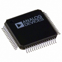
AD7606BSTZ-6RL Analog Devices Inc, AD7606BSTZ-6RL Datasheet - Page 32

AD7606BSTZ-6RL
Manufacturer Part Number
AD7606BSTZ-6RL
Description
Simulat Sampliing Bipolar 16 Bit I.C.
Manufacturer
Analog Devices Inc
Type
Data Acquisition System (DAS), ADCr
Datasheet
1.AD7606BSTZ-6.pdf
(36 pages)
Specifications of AD7606BSTZ-6RL
Design Resources
Layout Considerations for an Expandable Multichannel Simultaneous Sampling Data Acquisition System Based on AD7606 (CN0148)
Resolution (bits)
16 b
Sampling Rate (per Second)
200k
Data Interface
DSP, MICROWIRE™, Parallel, QSPI™, Serial, SPI™
Voltage Supply Source
Single Supply
Voltage - Supply
4.75 V ~ 5.25 V
Operating Temperature
-40°C ~ 85°C
Mounting Type
Surface Mount
Package / Case
64-LFQFP
Lead Free Status / RoHS Status
Lead free / RoHS Compliant
Other names
AD7606BSTZ-6RL
Available stocks
Company
Part Number
Manufacturer
Quantity
Price
Company:
Part Number:
AD7606BSTZ-6RL
Manufacturer:
ADI
Quantity:
1 359
Company:
Part Number:
AD7606BSTZ-6RL
Manufacturer:
Analog Devices Inc
Quantity:
10 000
AD7606/AD7606-6/AD7606-4
LAYOUT GUIDELINES
The printed circuit board that houses the AD7606/AD7606-6/
AD7606-4 should be designed so that the analog and digital
sections are separated and confined to different areas of the board.
At least one ground plane should be used. It can be common or
split between the digital and analog sections. In the case of the
split plane, the digital and analog ground planes should be
joined in only one place, preferably as close as possible to the
AD7606/AD7606-6/AD7606-4.
If the AD7606/AD7606-6/AD7606-4 are in a system where
multiple devices require analog-to-digital ground connections,
the connection should still be made at only one point: a star
ground point
AD7606/AD7606-6/AD7606-4. Good connections should be
made to the ground plane. Avoid sharing one connection for
multiple ground pins. Use individual vias or multiple vias to the
ground plane for each ground pin.
Avoid running digital lines under the devices because doing so
couples noise onto the die. The analog ground plane should be
allowed to run under the AD7606/AD7606-6/AD7606-4 to
avoid noise coupling. Fast switching signals like CONVST A,
CONVST B, or clocks should be shielded with digital ground
to avoid radiating noise to other sections of the board, and they
should never run near analog signal paths. Avoid crossover of
digital and analog signals. Traces on layers in close proximity on
the board should run at right angles to each other to reduce the
effect of feedthrough through the board.
The power supply lines to the AV
AD7606/AD7606-6/AD7606-4 should use as large a trace as
possible to provide low impedance paths and reduce the effect
of glitches on the power supply lines. Where possible, use supply
planes and make good connections between the AD7606 supply
pins and the power tracks on the board. Use a single via or multiple
vias for each supply pin.
Good decoupling is also important to lower the supply impedance
presented to the AD7606/AD7606-6/AD7606-4 and to reduce
the magnitude of the supply spikes. The decoupling capacitors
should be placed close to (ideally, right up against) these pins
and their corresponding ground pins. Place the decoupling
capacitors for the REFIN/REFOUT pin and the REFCAPA and
REFCAPB pins as close as possible to their respective AD7606/
AD7606-6/AD7606-4 pins; and, where possible, they should be
placed on the same side of the board as the AD7606 device.
that should be established as close as p
CC
and V
DRIVE
pins on the
ossible to the
Rev. A | Page 32 of 36
Figure 62 shows the recommended decoupling on the top layer
of the AD7606 board. Figure 63 shows bottom layer decoupling,
which is used for the four AV
Where the ceramic 100 nF caps for the AV
close to their respective device pins, a single 100 nF capacitor
can be shared between Pin 37 and Pin 38.
Figure 62. Top Layer Decoupling REFIN/REFOUT,
REFCAPA, REFCAPB, and REGCAP Pins
Figure 63. Bottom Layer Decoupling
CC
pins and the V
CC
DRIVE
pins are placed
pin decoupling.


