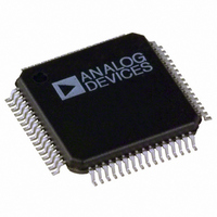
AD7606BSTZ-6RL Analog Devices Inc, AD7606BSTZ-6RL Datasheet - Page 22

AD7606BSTZ-6RL
Manufacturer Part Number
AD7606BSTZ-6RL
Description
Simulat Sampliing Bipolar 16 Bit I.C.
Manufacturer
Analog Devices Inc
Type
Data Acquisition System (DAS), ADCr
Datasheet
1.AD7606BSTZ-6.pdf
(36 pages)
Specifications of AD7606BSTZ-6RL
Design Resources
Layout Considerations for an Expandable Multichannel Simultaneous Sampling Data Acquisition System Based on AD7606 (CN0148)
Resolution (bits)
16 b
Sampling Rate (per Second)
200k
Data Interface
DSP, MICROWIRE™, Parallel, QSPI™, Serial, SPI™
Voltage Supply Source
Single Supply
Voltage - Supply
4.75 V ~ 5.25 V
Operating Temperature
-40°C ~ 85°C
Mounting Type
Surface Mount
Package / Case
64-LFQFP
Lead Free Status / RoHS Status
Lead free / RoHS Compliant
Other names
AD7606BSTZ-6RL
Available stocks
Company
Part Number
Manufacturer
Quantity
Price
Company:
Part Number:
AD7606BSTZ-6RL
Manufacturer:
ADI
Quantity:
1 359
Company:
Part Number:
AD7606BSTZ-6RL
Manufacturer:
Analog Devices Inc
Quantity:
10 000
AD7606/AD7606-6/AD7606-4
THEORY OF OPERATION
CONVERTER DETAILS
The AD7606/AD7606-6/AD7606-4 are data acquisition systems
that employ a high speed, low power, charge redistribution,
successive approximation analog-to-digital converter (ADC)
and allow the simultaneous sampling of eight/six/four analog input
channels. The analog inputs on the AD7606/AD7606-6/AD7606-4
can accept true bipolar input signals. The RANGE pin is used to
select either ±10 V or ±5 V as the input range. The AD7606/
AD7606-6/AD7606-4 operate from a single 5 V supply.
The AD7606/AD7606-6/AD7606-4 contain input clamp
protection, input signal scaling amplifiers, a second-order anti-
aliasing filter, track-and-hold amplifiers, an on-chip reference,
reference buffers, a high speed ADC, a digital filter, and high
speed parallel and serial interfaces. Sampling on the AD7606/
AD7606-6/AD7606-4 is controlled using the CONVST signals.
ANALOG INPUT
Analog Input Ranges
The AD7606/AD7606-6/AD7606-4 can handle true bipolar,
single-ended input voltages. The logic level on the RANGE pin
determines the analog input range of all analog input channels.
If this pin is tied to a logic high, the analog input range is ±10 V
for all channels. If this pin is tied to a logic low, the analog input
range is ±5 V for all channels. A logic change on this pin has an
immediate effect on the analog input range; however, there is
typically a settling time of approximately 80 μs, in addition to
the normal acquisition time requirement. The recommended
practice is to hardwire the RANGE pin according to the desired
input range for the system signals.
Analog Input Impedance
The analog input impedance of the AD7606/AD7606-6/
AD7606-4 is 1 MΩ. This is a fixed input impedance that does
not vary with the AD7606 sampling frequency. This high analog
input impedance eliminates the need for a driver amplifier in
front of the AD7606/AD7606-6/AD7606-4, allowing for direct
connection to the source or sensor. With the need for a driver
amplifier eliminated, bipolar supplies (which are often a source
of noise in a system) can be removed from the signal chain.
Rev. A | Page 22 of 36
Analog Input Clamp Protection
Figure 34 shows the analog input structure of the AD7606/
AD7606-6/AD7606-4. Each analog input of the AD7606/
AD7606-6/AD7606-4 contains clamp protection circuitry.
Despite single 5 V supply operation, this analog input clamp
protection allows for an input over voltage of up to ±16.5 V.
Figure 35 shows the voltage vs. current characteristic of the
clamp circuit. For input voltages of up to ±16.5 V, no current
flows in the clamp circuit. For input voltages that are above ±16.5 V,
the AD7606/AD7606-6/AD7606-4 clamp circuitry turns on.
A series resistor should be placed on the analog input channels
to limit the current to ±10 mA for input voltages above ±16.5 V.
In an application where there is a series resistance on an analog
input channel, Vx, a corresponding resistance is required on the
analog input GND channel, VxGND (see Figure 36). If there is
no corresponding resistor on the VxGND channel, an offset
error occurs on that channel.
VxGND
ANALOG
Figure 36. Input Resistance Matching on the Analog Input of the
SIGNAL
–10
–20
–30
–40
–50
INPUT
30
20
10
Vx
0
–20
AV
T
A
CC
= 25°C
–15
CLAMP
CLAMP
, V
Figure 35. Input Protection Clamp Profile
R
R
DRIVE
Figure 34. Analog Input Circuitry
C
AD7606/AD7606-6/AD7606-4
–10
= 5V
1MΩ
1MΩ
VxGND
SOURCE VOLTAGE (V)
Vx
–5
R
R
FB
FB
AD7606
CLAMP
CLAMP
0
SECOND-
ORDER
LPF
5
1MΩ
1MΩ
10
R
R
FB
FB
15
20


