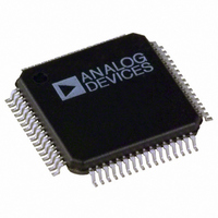
AD7606BSTZ-6RL Analog Devices Inc, AD7606BSTZ-6RL Datasheet - Page 15

AD7606BSTZ-6RL
Manufacturer Part Number
AD7606BSTZ-6RL
Description
Simulat Sampliing Bipolar 16 Bit I.C.
Manufacturer
Analog Devices Inc
Type
Data Acquisition System (DAS), ADCr
Datasheet
1.AD7606BSTZ-6.pdf
(36 pages)
Specifications of AD7606BSTZ-6RL
Design Resources
Layout Considerations for an Expandable Multichannel Simultaneous Sampling Data Acquisition System Based on AD7606 (CN0148)
Resolution (bits)
16 b
Sampling Rate (per Second)
200k
Data Interface
DSP, MICROWIRE™, Parallel, QSPI™, Serial, SPI™
Voltage Supply Source
Single Supply
Voltage - Supply
4.75 V ~ 5.25 V
Operating Temperature
-40°C ~ 85°C
Mounting Type
Surface Mount
Package / Case
64-LFQFP
Lead Free Status / RoHS Status
Lead free / RoHS Compliant
Other names
AD7606BSTZ-6RL
Available stocks
Company
Part Number
Manufacturer
Quantity
Price
Company:
Part Number:
AD7606BSTZ-6RL
Manufacturer:
ADI
Quantity:
1 359
Company:
Part Number:
AD7606BSTZ-6RL
Manufacturer:
Analog Devices Inc
Quantity:
10 000
Pin No.
22 to 16
23
24
25
31 to 27
32
33
34
36, 39
42
Type
DO
P
DO
DO
DO
DO/DI
DO/DI
DI
P
REF
1
DB[6:0]
V
DB7/D
DB8/D
DB[13:9]
DB14/
HBEN
DB15/
BYTE SEL
REF SELECT
REGCAP
REFIN/
REFOUT
AD7606
DRIVE
OUT
OUT
A
B
Mnemonic
DB[6:0]
V
DB7/D
DB8/D
DB[13:9]
DB14/
HBEN
DB15/
BYTE SEL
REF SELECT
REGCAP
REFIN/
REFOUT
AD7606-6
DRIVE
OUT
OUT
A
B
DB[6:0]
V
DB7/D
DB8/D
DB[13:9]
DB14/
HBEN
DB15/
BYTE SEL
REF SELECT
REGCAP
REFIN/
REFOUT
AD7606-4
DRIVE
OUT
OUT
Rev. A | Page 15 of 36
A
B
Description
Parallel Output Data Bits, DB6 to DB0. When PAR/SER/BYTE SEL = 0, these
pins act as three-state parallel digital input/output pins. When CS and RD
are low, these pins are used to output DB6 to DB0 of the conversion result.
When PAR/SER/BYTE SEL = 1, these pins should be tied to AGND. When
operating in parallel byte interface mode, DB[7:0] outputs the 16-bit con-
version result in two RD operations. DB7 (Pin 24) is the MSB; DB0 is the LSB.
Logic Power Supply Input. The voltage (2.3 V to 5.25 V) supplied at this pin
determines the operating voltage of the interface. This pin is nominally at the
same supply as the supply of the host interface (that is, DSP and FPGA).
Parallel Output Data Bit 7 (DB7)/Serial Interface Data Output Pin (D
When PAR/SER/BYTE SEL = 0, this pins acts as a three-state parallel digital
input/output pin. When CS and RD are low, this pin is used to output DB7
of the conversion result. When PAR/SER/BYTE SEL = 1, this pin functions
as D
section for more details). When operating in parallel byte mode, DB7 is
the MSB of the byte.
Parallel Output Data Bit 8 (DB8)/Serial Interface Data Output Pin (D
When PAR/SER/BYTE SEL = 0, this pin acts as a three-state parallel digital
input/output pin. When CS and RD are low, this pin is used to output
DB8 of the conversion result. When PAR/SER/BYTE SEL = 1, this pin functions
as D
section for more details).
Parallel Output Data Bits, DB13 to DB9. When PAR/SER/BYTE SEL = 0, these
pins act as three-state parallel digital input/output pins. When CS and RD
are low, these pins are used to output DB13 to DB9 of the conversion result.
When PAR/SER/BYTE SEL = 1, these pins should be tied to AGND.
Parallel Output Data Bit 14 (DB14)/High Byte Enable (HBEN). When PAR/
SER/BYTE SEL = 0, this pin acts as a three-state parallel digital output pin.
When CS and RD are low, this pin is used to output DB14 of the conversion
result. When PAR/SER/BYTE SEL = 1 and DB15/BYTE SEL = 1, the AD7606/
AD7606-6/AD7606-4 operate in parallel byte interface mode. In parallel
byte mode, the HBEN pin is used to select whether the most significant byte
(MSB) or the least significant byte (LSB) of the conversion result is output first.
When HBEN = 1, the MSB is output first, followed by the LSB.
When HBEN = 0, the LSB is output first, followed by the MSB.
Parallel Output Data Bit 15 (DB15)/Parallel Byte Mode Select (BYTE SEL).
When PAR/SER/BYTE SEL = 0, this pin acts as a three-state parallel digital
output pin. When CS and RD are low, this pin is used to output DB15 of the
conversion result. When PAR/SER/BYTE SEL = 1, the BYTE SEL pin is used to
select between serial interface mode and parallel byte interface mode
(see
AD7606 operates in serial interface mode. When PAR/SER/BYTE SEL = 1
and DB15/BYTE SEL = 1, the AD7606 operates in parallel byte interface mode.
Internal/External Reference Selection Input. Logic input. If this pin is set to
logic high, the internal reference is selected and enabled. If this pin is set to
logic low, the internal reference is disabled and an external reference
voltage must be applied to the REFIN/REFOUT pin.
Decoupling Capacitor Pin for Voltage Output from Internal Regulator.
These output pins should be decoupled separately to AGND using a 1 μF
capacitor. The voltage on these pins is in the range of 2.5 V to 2.7 V.
Reference Input (REFIN)/Reference Output (REFOUT). The on-chip reference
of 2.5 V is available on this pin for external use if the REF SELECT pin is set to
logic high. Alternatively, the internal reference can be disabled by setting
the REF SELECT pin to logic low, and an external reference of 2.5 V can be
applied to this input (see the Internal/External Reference section).
Decoupling is required on this pin for both the internal and external
reference options. A 10 μF capacitor should be applied from this pin to
ground close to the REFGND pins.
OUT
OUT
Table 8
A and outputs serial conversion data (see the
B and outputs serial conversion data (see the
). When
PAR/SER/BYTE SEL = 1 and DB15/BYTE SEL = 0, the
AD7606/AD7606-6/AD7606-4
Conversion Control
Conversion Control
OUT
OUT
A).
B).


