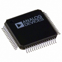
AD7606BSTZ-6RL Analog Devices Inc, AD7606BSTZ-6RL Datasheet - Page 29

AD7606BSTZ-6RL
Manufacturer Part Number
AD7606BSTZ-6RL
Description
Simulat Sampliing Bipolar 16 Bit I.C.
Manufacturer
Analog Devices Inc
Type
Data Acquisition System (DAS), ADCr
Datasheet
1.AD7606BSTZ-6.pdf
(36 pages)
Specifications of AD7606BSTZ-6RL
Design Resources
Layout Considerations for an Expandable Multichannel Simultaneous Sampling Data Acquisition System Based on AD7606 (CN0148)
Resolution (bits)
16 b
Sampling Rate (per Second)
200k
Data Interface
DSP, MICROWIRE™, Parallel, QSPI™, Serial, SPI™
Voltage Supply Source
Single Supply
Voltage - Supply
4.75 V ~ 5.25 V
Operating Temperature
-40°C ~ 85°C
Mounting Type
Surface Mount
Package / Case
64-LFQFP
Lead Free Status / RoHS Status
Lead free / RoHS Compliant
Other names
AD7606BSTZ-6RL
Available stocks
Company
Part Number
Manufacturer
Quantity
Price
Company:
Part Number:
AD7606BSTZ-6RL
Manufacturer:
ADI
Quantity:
1 359
Company:
Part Number:
AD7606BSTZ-6RL
Manufacturer:
Analog Devices Inc
Quantity:
10 000
DIGITAL FILTER
The AD7606/AD7606-6/AD7606-4 contain an optional digital
first-order sinc filter that should be used in applications where
slower throughput rates are used or where higher signal-to-noise
ratio or dynamic range is desirable. The oversampling ratio of the
digital filter is controlled using the oversampling pins, OS [2:0] (see
Table 9). OS 2 is the MSB control bit, and OS 0 is the LSB control
bit. Table 9 provides the oversampling bit decoding to select the
different oversample rates. The OS pins are latched on the falling
edge of BUSY. This sets the oversampling rate for the next
conversion (see Figure 48). In addition to the oversampling
function, the output result is decimated to 16-bit resolution.
If the OS pins are set to select an OS ratio of eight, the next
CONVST x rising edge takes the first sample for each channel,
and the remaining seven samples for all channels are taken with
an internally generated sampling signal. These samples are then
averaged to yield an improvement in SNR performance. Table 9
shows typical SNR performance for both the ±10 V and the ±5 V
range. As Table 9 shows, there is an improvement in SNR as the
OS ratio increases. As the OS ratio increases, the 3 dB frequency
is reduced, and the allowed sampling frequency is also reduced.
In an application where the required sampling frequency is
10 kSPS, an OS ratio of up to 16 can be used. In this case, the
application sees an improvement in SNR, but the input 3 dB
bandwidth is limited to ~6 kHz.
The CONVST A and CONVST B pins must be tied/driven
together when oversampling is turned on. When the over-
sampling function is turned on, the BUSY high time for the
conversion process extends. The actual BUSY high time
depends on the oversampling rate that is selected: the higher the
oversampling rate, the longer the BUSY high, or total conversion
time (see Table 3).
Table 9. Oversample Bit Decoding
OS[2:0]
000
001
010
011
100
101
110
111
OS
Ratio
No OS
2
4
8
16
32
64
Invalid
SNR 5 V Range
(dB)
89
91.2
92.6
94.2
95.5
96.4
96.9
CONVST A
CONVST B
BUSY
OS x
AND
SNR 10 V Range
(dB)
90
92
93.6
95
96
96.7
97
t
OS_SETUP
CONVERSION N
Figure 48. OS x Pin Timing
3 dB BW 5 V Range
(kHz)
15
15
13.7
10.3
6
3
1.5
OVERSAMPLE RATE
LATCHED FOR CONVERSION N + 1
Rev. A | Page 29 of 36
t
OS_HOLD
Figure 47 shows that the conversion time extends as the over-
sampling rate is increased, and the BUSY signal lengthens for the
different oversampling rates. For example, a sampling frequency
of 10 kSPS yields a cycle time of 100 μs. Figure 47 shows OS × 2
and OS × 4; for a 10 kSPS example, there is adequate cycle time to
further increase the oversampling rate and yield greater improve-
ments in SNR performance. In an application where the initial
sampling or throughput rate is at 200 kSPS, for example, and
oversampling is turned on, the throughput rate must be reduced
to accommodate the longer conversion time and to allow for the
read. To achieve the fastest throughput rate possible when over-
sampling is turned on, the read can be performed during the
BUSY high time. The falling edge of BUSY is used to update the
output data registers with the new conversion data; therefore, the
reading of conversion data should not occur on this edge.
CONVST A
CONVST B
DB[15:0]
DATA:
BUSY
AND
Figure 47. AD7606—No Oversampling, Oversampling × 2, and
RD
CS
3 dB BW 10 V Range
(kHz)
22
22
18.5
11.9
6
3
1.5
Oversampling × 4 While Using Read After Conversion
OS = 0 OS = 2 OS = 4
4µs
AD7606/AD7606-6/AD7606-4
CONVERSION N + 1
9µs
t
CONV
19µs
t
4
t
4
t
4
Maximum Throughput
CONVST Frequency (kHz)
100
50
25
12.5
6.25
3.125
200
t
CYCLE


