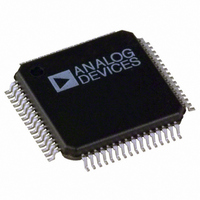
AD7606BSTZ-6RL Analog Devices Inc, AD7606BSTZ-6RL Datasheet - Page 9

AD7606BSTZ-6RL
Manufacturer Part Number
AD7606BSTZ-6RL
Description
Simulat Sampliing Bipolar 16 Bit I.C.
Manufacturer
Analog Devices Inc
Type
Data Acquisition System (DAS), ADCr
Datasheet
1.AD7606BSTZ-6.pdf
(36 pages)
Specifications of AD7606BSTZ-6RL
Design Resources
Layout Considerations for an Expandable Multichannel Simultaneous Sampling Data Acquisition System Based on AD7606 (CN0148)
Resolution (bits)
16 b
Sampling Rate (per Second)
200k
Data Interface
DSP, MICROWIRE™, Parallel, QSPI™, Serial, SPI™
Voltage Supply Source
Single Supply
Voltage - Supply
4.75 V ~ 5.25 V
Operating Temperature
-40°C ~ 85°C
Mounting Type
Surface Mount
Package / Case
64-LFQFP
Lead Free Status / RoHS Status
Lead free / RoHS Compliant
Other names
AD7606BSTZ-6RL
Available stocks
Company
Part Number
Manufacturer
Quantity
Price
Company:
Part Number:
AD7606BSTZ-6RL
Manufacturer:
ADI
Quantity:
1 359
Company:
Part Number:
AD7606BSTZ-6RL
Manufacturer:
Analog Devices Inc
Quantity:
10 000
Parameter
1
2
3
4
Timing Diagrams
Sample tested during initial release to ensure compliance. All input signals are specified with t
In oversampling mode, typical t
t
The delay between the CONVST x signals was measured as the maximum time allowed while ensuring a <10 LSB performance matching between channel sets.
A buffer is used on the data output pins for these measurements, which is equivalent to a load of 20 pF on the output pins.
CONV
t
t
t
27
28
29
= 3 μs; and for the AD7606-4, t
CONVST A,
CONVST A,
CONVST A,
CONVST A,
FRSTDATA
CONVST B
CONVST B
CONVST B
CONVST B
DB[15:0]
RESET
RESET
DATA:
BUSY
BUSY
RD
CS
CS
CS
CONV
for the AD7606-6 and AD7606-4 can be calculated using ((N × t
CONV
Min
= 2 μs.
INVALID
t
Limit at T
t
8
13
t
24
t
26
t
t
t
1
7
7
Typ
t
t
t
RESET
RESET
10
t
t
Figure 3. CONVST Timing—Reading During a Conversion
5
5
MIN
Figure 2. CONVST Timing—Reading After a Conversion
V1
Figure 4. Parallel Mode, Separate CS and RD Pulses
, T
MAX
Max
19
24
17
22
24
t
1
t
t
11
27
V2
Unit
ns
ns
ns
ns
ns
Rev. A | Page 9 of 36
Delay from RD falling edge to FRSTDATA low
V
V
Delay from 16
V
V
Delay from CS rising edge until FRSTDATA three-state enabled
Description
V3
t
DRIVE
DRIVE
DRIVE
DRIVE
14
= 3.3 V to 5.25V
= 2.3 V to 2.7V
= 3.3 V to 5.25V
= 2.3 V to 2.7V
t
t
t
t
CYCLE
CYCLE
CONV
CONV
V4
t
t
3
3
R
= t
CONV
th
F
= 5 ns (10% to 90% of V
SCLK falling edge to FRSTDATA low
) + ((N − 1) × 1 μs)). N is the oversampling ratio. For the AD7606-6,
t
6
V7
t
AD7606/AD7606-6/AD7606-4
15
t
4
DRIVE
V8
) and timed from a voltage level of 1.6 V.
t
t
t
16
17
29
t
9
t
t
2
2


