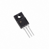
STGF10NB60SD STMicroelectronics, STGF10NB60SD Datasheet - Page 5

STGF10NB60SD
Manufacturer Part Number
STGF10NB60SD
Description
MOSFET N-CHAN 10A 600V TO-220FP
Manufacturer
STMicroelectronics
Series
PowerMESH™r
Datasheet
1.STGP10NB60SD.pdf
(15 pages)
Specifications of STGF10NB60SD
Voltage - Collector Emitter Breakdown (max)
600V
Vce(on) (max) @ Vge, Ic
1.8V @ 15V, 10A
Current - Collector (ic) (max)
20A
Power - Max
25W
Input Type
Standard
Mounting Type
Through Hole
Package / Case
TO-220-3 Full Pack (Straight Leads)
Transistor Type
IGBT
Dc Collector Current
20A
Collector Emitter Voltage Vces
1.8V
Power Dissipation Pd
25W
Collector Emitter Voltage V(br)ceo
600V
Operating Temperature Range
-55°C To +150°C
Rohs Compliant
Yes
Lead Free Status / RoHS Status
Lead free / RoHS Compliant
Igbt Type
-
Available stocks
Company
Part Number
Manufacturer
Quantity
Price
Part Number:
STGF10NB60SD
Manufacturer:
ST
Quantity:
20 000
STGF10NB60SD, STGP10NB60SD
Table 6.
Table 7.
1. Eon is the turn-on losses when a typical diode is used in the test circuit. If the IGBT is offered in a package
2. Turn-off losses include also the tail of the collector current.
Table 8.
Symbol
(di/dt)
Symbol
Symbol
t
t
Eon
E
E
t
t
t
r
r
with a co-pack diode, the co-pack diode is used as external diode. IGBTs and diode are at the same
temperature (25°C and 125°C)
d
d
d(on)
(V
(V
off
off
E
I
I
(
(
Q
Q
V
t
t
t
rrm
rrm
t
t
off
off
r
f
f
off
off
rr
rr
ts
F
rr
rr
(2)
(2)
(1)
on
)
)
)
)
Turn-on delay time
Current rise time
Turn-on current slope
Off voltage rise time
Turn-off delay time
Current fall time
Off voltage rise time
Turn-off delay time
Current fall time
Turn-on switching losses
Turn-off switching losses
Total switching losses
Turn-off switching losses
Forward on-voltage
Reverse recovery time
Reverse recovery charge
Reverse recovery current
Reverse recovery time
Reverse recovery charge
Reverse recovery current
Switching on/off (inductive load)
Switching energy (inductive load)
Collector-emitter diode
Parameter
Parameter
Parameter
Doc ID 11860 Rev 2
I
I
I
di/dt = 100 A/µs
(see Figure 21)
I
T
di/dt = 100 A/µs
(see Figure 21)
F
F
F
F
V
R
(see Figure 18)
V
R
(see Figure 18)
V
R
T
(see Figure 18)
V
R
(see Figure 18)
V
R
T
(see Figure 18)
j
= 125 °C,
= 10 A
= 10 A, T
= 7 A, V
= 7 A, V
j
j
CC
CC
CC
CC
CC
G
G
G
G
G
= 125 °C
= 125 °C
= 1 kΩ , V
= 1 kΩ , V
= 1 kΩ , V
= 1 kΩ , V
= 1 kΩ , V
Test conditions
= 480 V, I
= 480 V, I
= 480 V, I
= 480 V, I
= 480 V, I
Test conditions
Test conditions
R
R
C
= 40 V,
= 40 V,
= 125 °C
GE
GE
GE
GE
GE
C
C
C
C
C
= 15 V
= 15 V
= 15 V,
= 15 V
= 15 V,
= 10 A
= 10 A
= 10 A
= 10 A
= 10 A
Electrical characteristics
Min.
Min.
Min
-
-
-
-
-
Typ.
1.4
2.1
3.2
Typ. Max.
Typ.
0.46
37
40
61
98
0.6
5.6
0.7
2.2
1.2
1.2
3.8
1.2
1.9
5
8
8
Max
Max. Unit
2.2
-
-
-
-
-
A/µs
Unit
Unit
nC
nC
µs
µs
µs
µs
µJ
µJ
µJ
µJ
ns
ns
V
V
A
A
5/15


