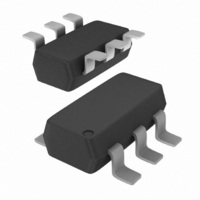
PMN50XP,165 NXP Semiconductors, PMN50XP,165 Datasheet

PMN50XP,165
Specifications of PMN50XP,165
PMN50XP /T2
PMN50XP /T2
Available stocks
Related parts for PMN50XP,165
PMN50XP,165 Summary of contents
Page 1
PMN50XP P-channel TrenchMOS extremely low level FET Rev. 02 — 2 October 2007 1. Product profile 1.1 General description Extremely low level P-channel enhancement mode Field-Effect Transistor (FET plastic package. This product is designed and qualified for use ...
Page 2
... NXP Semiconductors 2. Pinning information Table 2. Pinning Pin Symbol Description 1 D drain 2 D drain 3 G gate 4 S source 5 D drain 6 D drain 3. Ordering information Table 3. Ordering information Type number Package Name Description PMN50XP TSOP6 plastic surface-mounted package (TSOP6); 6 leads 4. Limiting values Table 4. ...
Page 3
... NXP Semiconductors 120 I der (%) 100 × 100 % der 25°C ) Fig 1. Normalized continuous drain current as a function of solder point temperature − (A) Limit R DSon −10 −1 −1 −10 −1 − ° single pulse Fig 3. Safe operating area; continuous and peak drain currents as a function of drain-source voltage ...
Page 4
... NXP Semiconductors 5. Thermal characteristics Table 5. Thermal characteristics Symbol Parameter R thermal resistance th(j-sp) from junction to solder point th(j-sp) δ = 0.5 (K/W) 0.2 10 0.1 0.05 0.02 single pulse Fig 4. Transient thermal impedance from junction to solder point as a function of pulse duration 6. Characteristics Table 6. Characteristics ...
Page 5
... NXP Semiconductors Table 6. Characteristics …continued Symbol Parameter I gate leakage current GSS R drain-source on-state DSon resistance Dynamic characteristics Q total gate charge G(tot) Q gate-source charge GS Q gate-drain charge GD C input capacitance iss C output capacitance oss C reverse transfer rss capacitance t turn-on delay time d(on) ...
Page 6
... NXP Semiconductors -1.2 V GS(th) max (V) -0.8 typ min -0 Fig 5. Gate-source threshold voltage as a function of junction temperature 150 - DSon (mΩ) 120 - °C j Fig 7. Drain-source on-state resistance as a function of drain current; typical values PMN50XP_2 Product data sheet P-channel TrenchMOS extremely low level FET 03ar95 − ...
Page 7
... NXP Semiconductors - -4 ° ° Fig 9. Gate-source voltage as a function of gate charge; typical values Fig 11. Input, output and reverse transfer capacitances as a function of drain-source voltage; typical values PMN50XP_2 Product data sheet P-channel TrenchMOS extremely low level FET 03aq09 (nC) G Fig 10. Gate charge waveform definitions ...
Page 8
... NXP Semiconductors 7. Package outline Plastic surface-mounted package (TSOP6); 6 leads pin 1 index 1 e DIMENSIONS (mm are the original dimensions) UNIT 0.1 0.40 1.1 0.26 mm 0.013 0.25 0.10 0.9 OUTLINE VERSION IEC SOT457 Fig 12. Package outline SOT457 (TSOP6) PMN50XP_2 Product data sheet P-channel TrenchMOS extremely low level FET ...
Page 9
... Document ID Release date PMN50XP_2 20071002 • Modifications: The format of this data sheet has been redesigned to comply with the new identity guidelines of NXP Semiconductors. • Legal texts have been adapted to the company name where appropriate. PMN50XP_1 20060123 PMN50XP_2 Product data sheet P-channel TrenchMOS extremely low level FET ...
Page 10
... For detailed and full information see the relevant full data sheet, which is available on request via the local NXP Semiconductors sales office. In case of any inconsistency or conflict with the short data sheet, the full data sheet shall prevail ...
Page 11
... NXP Semiconductors 11. Contents 1 Product profile . . . . . . . . . . . . . . . . . . . . . . . . . . 1 1.1 General description . . . . . . . . . . . . . . . . . . . . . 1 1.2 Features . . . . . . . . . . . . . . . . . . . . . . . . . . . . . . 1 1.3 Applications . . . . . . . . . . . . . . . . . . . . . . . . . . . 1 1.4 Quick reference data . . . . . . . . . . . . . . . . . . . . 1 2 Pinning information . . . . . . . . . . . . . . . . . . . . . . 2 3 Ordering information . . . . . . . . . . . . . . . . . . . . . 2 4 Limiting values Thermal characteristics . . . . . . . . . . . . . . . . . . 4 6 Characteristics . . . . . . . . . . . . . . . . . . . . . . . . . . 4 7 Package outline . . . . . . . . . . . . . . . . . . . . . . . . . 8 8 Revision history . . . . . . . . . . . . . . . . . . . . . . . . . 9 9 Legal information 9.1 Data sheet status . . . . . . . . . . . . . . . . . . . . . . 10 9 ...


