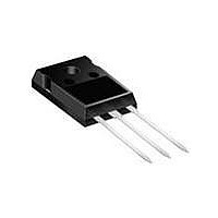
STW30N65M5 STMicroelectronics, STW30N65M5 Datasheet - Page 4

STW30N65M5
Manufacturer Part Number
STW30N65M5
Description
MOSFET N-CH 650V 22A TO-247
Manufacturer
STMicroelectronics
Series
MDmesh™r
Datasheet
1.STP30N65M5.pdf
(18 pages)
Specifications of STW30N65M5
Fet Type
MOSFET N-Channel, Metal Oxide
Fet Feature
Standard
Rds On (max) @ Id, Vgs
139 mOhm @ 11A, 10V
Drain To Source Voltage (vdss)
650V
Current - Continuous Drain (id) @ 25° C
22A
Vgs(th) (max) @ Id
5V @ 250µA
Gate Charge (qg) @ Vgs
64nC @ 10V
Input Capacitance (ciss) @ Vds
2880pF @ 100V
Power - Max
140W
Mounting Type
Through Hole
Package / Case
TO-247
Configuration
Single
Transistor Polarity
N-Channel
Resistance Drain-source Rds (on)
0.139 Ohms
Drain-source Breakdown Voltage
650 V
Gate-source Breakdown Voltage
3 V
Continuous Drain Current
22 A
Power Dissipation
140 W
Maximum Operating Temperature
+ 150 C
Mounting Style
Through Hole
Gate Charge Qg
64 nC
Lead Free Status / RoHS Status
Lead free / RoHS Compliant
Other names
497-10655-5
STW30N65M5
STW30N65M5
Electrical characteristics
2
4/18
Electrical characteristics
(T
Table 4.
Table 5.
1. C
2. C
V
Symbol
Symbol
C
C
R
C
V
(BR)DSS
when V
C
C
o(er)
I
I
C
DS(on)
C
o(tr)
Q
GS(th)
Q
= 25 °C unless otherwise specified)
GSS
R
DSS
Q
oss eq.
oss eq.
oss
oss
iss
rss
gs
gd
G
g
(1)
(2)
when V
DS
time related is defined as a constant equivalent capacitance giving the same charging time as C
energy related is defined as a constant equivalent capacitance giving the same stored energy as
Input capacitance
Output capacitance
Reverse transfer
capacitance
Equivalent
capacitance time
related
Equivalent
capacitance energy
related
Intrinsic gate
resistance
Total gate charge
Gate-source charge
Gate-drain charge
increases from 0 to 80% V
Drain-source
breakdown voltage
Zero gate voltage
drain current (V
Gate-body leakage
current (V
Gate threshold voltage V
Static drain-source on
resistance
On /off states
Dynamic
DS
increases from 0 to 80% V
Parameter
Parameter
DS
= 0)
GS
= 0)
Doc ID 15331 Rev 2
DSS
V
V
V
V
f = 1 MHz open drain
V
V
(see
I
V
V
V
V
D
DS
GS
GS
GS
DD
GS
DS
DS
GS
DS
GS
= 1 mA, V
DSS
= Max rating
= Max rating, T
= 100 V, f = 1 MHz,
= 0
= 0, V
= 0, V
= 10 V
= ± 25 V
= V
= 10 V, I
= 520 V, I
Figure
Test conditions
Test conditions
GS
DS
DS
, I
20)
GS
D
D
= 0 to 520 V
= 0 to 520 V
D
= 250 µA
= 11 A
= 0
= 11 A,
C
=125 °C
Min.
Min.
650
3
-
-
-
-
-
STB/F/I/P/W30N65M5
0.125
2880
Typ.
Typ.
189
319
1.6
68
64
16
25
4
5
0.139
Max.
Max.
100
100
1
5
-
-
-
-
-
oss
Unit
Unit
nC
nC
nC
µA
µA
nA
pF
pF
pF
pF
pF
Ω
Ω
V
V


