BFG541,115 NXP Semiconductors, BFG541,115 Datasheet - Page 6
BFG541,115
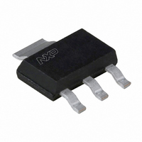
Manufacturer Part Number
BFG541,115
Description
TRANS NPN 15V 9GHZ SOT223
Manufacturer
NXP Semiconductors
Datasheet
1.BFG541115.pdf
(14 pages)
Specifications of BFG541,115
Package / Case
SOT-223 (3 leads + Tab), SC-73, TO-261
Transistor Type
NPN
Voltage - Collector Emitter Breakdown (max)
15V
Frequency - Transition
9GHz
Noise Figure (db Typ @ F)
1.3dB ~ 2.4dB @ 900MHz
Power - Max
650mW
Dc Current Gain (hfe) (min) @ Ic, Vce
60 @ 40mA, 8V
Current - Collector (ic) (max)
120mA
Mounting Type
Surface Mount
Dc Current Gain Hfe Max
60 @ 40mA @ 8V
Mounting Style
SMD/SMT
Configuration
Single Dual Emitter
Transistor Polarity
NPN
Maximum Operating Frequency
9000 MHz (Typ)
Collector- Emitter Voltage Vceo Max
15 V
Emitter- Base Voltage Vebo
2.5 V
Continuous Collector Current
0.12 A
Power Dissipation
650 mW
Maximum Operating Temperature
+ 175 C
Dc
08+
Lead Free Status / RoHS Status
Lead free / RoHS Compliant
Gain
-
Lead Free Status / Rohs Status
Lead free / RoHS Compliant
Other names
568-1984-2
934018870115
BFG541 T/R
934018870115
BFG541 T/R


NXP Semiconductors
In Figs 6 to 9, G
maximum stable gain; G
September 1995
handbook, halfpage
handbook, halfpage
NPN 9 GHz wideband transistor
V
I
C
CE
gain
(dB)
gain
(dB)
= 10 mA; V
Fig.6 Gain as a function of collector current.
= 8 V; f = 900 MHz.
25
20
15
10
50
40
30
20
10
5
0
0
10
0
Fig.8 Gain as a function of frequency.
MSG
CE
= 8 V.
UM
20
= maximum power gain; MSG =
MSG
10
2
G UM
max
G max
G UM
40
= maximum available gain.
10
3
G max
60
f (MHz)
I C (mA)
MRA660
MRA658
80
10
4
6
handbook, halfpage
handbook, halfpage
V
I
C
CE
gain
(dB)
gain
(dB)
= 40 mA; V
Fig.7 Gain as a function of collector current.
= 8 V; f = 2 GHz.
25
20
15
10
50
40
30
20
10
5
0
0
10
0
Fig.9 Gain as a function of frequency.
CE
= 8 V.
MSG
20
G UM
10
2
G max
G UM
40
10
3
Product specification
G max
60
f (MHz)
I C (mA)
BFG541
MRA659
MRA661
80
10
4
Related parts for BFG541,115
Image
Part Number
Description
Manufacturer
Datasheet
Request
R

Part Number:
Description:
Npn 9 Ghz Wideband Transistor
Manufacturer:
NXP Semiconductors
Datasheet:
Part Number:
Description:
Bfg541 Npn 9 Ghz Wideband Transistor
Manufacturer:
NXP Semiconductors
Datasheet:
Part Number:
Description:
NXP Semiconductors designed the LPC2420/2460 microcontroller around a 16-bit/32-bitARM7TDMI-S CPU core with real-time debug interfaces that include both JTAG andembedded trace
Manufacturer:
NXP Semiconductors
Datasheet:

Part Number:
Description:
NXP Semiconductors designed the LPC2458 microcontroller around a 16-bit/32-bitARM7TDMI-S CPU core with real-time debug interfaces that include both JTAG andembedded trace
Manufacturer:
NXP Semiconductors
Datasheet:
Part Number:
Description:
NXP Semiconductors designed the LPC2468 microcontroller around a 16-bit/32-bitARM7TDMI-S CPU core with real-time debug interfaces that include both JTAG andembedded trace
Manufacturer:
NXP Semiconductors
Datasheet:
Part Number:
Description:
NXP Semiconductors designed the LPC2470 microcontroller, powered by theARM7TDMI-S core, to be a highly integrated microcontroller for a wide range ofapplications that require advanced communications and high quality graphic displays
Manufacturer:
NXP Semiconductors
Datasheet:
Part Number:
Description:
NXP Semiconductors designed the LPC2478 microcontroller, powered by theARM7TDMI-S core, to be a highly integrated microcontroller for a wide range ofapplications that require advanced communications and high quality graphic displays
Manufacturer:
NXP Semiconductors
Datasheet:
Part Number:
Description:
The Philips Semiconductors XA (eXtended Architecture) family of 16-bit single-chip microcontrollers is powerful enough to easily handle the requirements of high performance embedded applications, yet inexpensive enough to compete in the market for hi
Manufacturer:
NXP Semiconductors
Datasheet:
Part Number:
Description:
The XA-S3 device is a member of Philips Semiconductors? XA(eXtended Architecture) family of high performance 16-bitsingle-chip microcontrollers
Manufacturer:
NXP Semiconductors
Datasheet:

Part Number:
Description:
The NXP BlueStreak LH75401/LH75411 family consists of two low-cost 16/32-bit System-on-Chip (SoC) devices
Manufacturer:
NXP Semiconductors
Datasheet:
Part Number:
Description:
The NXP LPC3130/3131 combine an 180 MHz ARM926EJ-S CPU core, high-speed USB2
Manufacturer:
NXP Semiconductors
Datasheet:
Part Number:
Description:
The NXP LPC3141 combine a 270 MHz ARM926EJ-S CPU core, High-speed USB 2
Manufacturer:
NXP Semiconductors
Part Number:
Description:
The NXP LPC3143 combine a 270 MHz ARM926EJ-S CPU core, High-speed USB 2
Manufacturer:
NXP Semiconductors

Part Number:
Description:
The NXP LPC3152 combines an 180 MHz ARM926EJ-S CPU core, High-speed USB 2
Manufacturer:
NXP Semiconductors