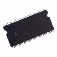
MT46V64M16P-6T:A Micron Technology Inc, MT46V64M16P-6T:A Datasheet - Page 46

MT46V64M16P-6T:A
Manufacturer Part Number
MT46V64M16P-6T:A
Description
DRAM Chip DDR SDRAM 1G-Bit 64Mx16 2.5V 66-Pin TSOP Tray
Manufacturer
Micron Technology Inc
Type
DDR SDRAMr
Datasheet
1.MT46V256M4P-6TA_TR.pdf
(82 pages)
Specifications of MT46V64M16P-6T:A
Density
1 Gb
Maximum Clock Rate
333 MHz
Package
66TSOP
Operating Supply Voltage
2.5 V
Maximum Random Access Time
0.7 ns
Operating Temperature
0 to 70 °C
Format - Memory
RAM
Memory Type
DDR SDRAM
Memory Size
1G (64M x 16)
Speed
6ns
Interface
Parallel
Voltage - Supply
2.3 V ~ 2.7 V
Package / Case
66-TSOP
Organization
64Mx16
Address Bus
16b
Access Time (max)
700ps
Operating Supply Voltage (typ)
2.5V
Package Type
TSOP
Operating Temp Range
0C to 70C
Operating Supply Voltage (max)
2.7V
Operating Supply Voltage (min)
2.3V
Supply Current
275mA
Pin Count
66
Mounting
Surface Mount
Operating Temperature Classification
Commercial
Lead Free Status / RoHS Status
Lead free / RoHS Compliant
Available stocks
Company
Part Number
Manufacturer
Quantity
Price
Company:
Part Number:
MT46V64M16P-6T:A
Manufacturer:
MICRON
Quantity:
5 530
Company:
Part Number:
MT46V64M16P-6T:A
Manufacturer:
MICRON
Quantity:
48
Part Number:
MT46V64M16P-6T:A
Manufacturer:
MICRON/美光
Quantity:
20 000
REGISTER DEFINITION
Mode Register
Figure 21:
PDF: 09005aef80a2f898/Source: 09005aef82a95a3a
DDR_x4x8x16_Core2.fm - 1Gb DDR: Rev. I, Core DDR: Rev. B 12/07 EN
Mode Register Definition
Notes:
The mode register is used to define the specific DDR SDRAM mode of operation. This
definition includes the selection of a burst length, a burst type, a CAS latency, and an
operating mode, as shown in Figure 21. The mode register is programmed via the LMR
command (with BA0 = 0 and BA1 = 0) and will retain the stored information until it is
programmed again or until the device loses power (except for bit A8, which is self-
clearing).
Reprogramming the mode register will not alter the contents of the memory, provided it
is performed correctly. The mode register must be loaded (reloaded) when all banks are
idle and no bursts are in progress, and the controller must wait the specified time before
initiating the subsequent operation. Violating either of these requirements will result in
unspecified operation.
Mode register bits A0–A2 specify the burst length, A3 specifies the type of burst (sequen-
tial or interleaved), A4–A6 specify the CAS latency, and A7–An specify the operating
mode.
1. n is the most significant row address bit from Table 2 on page 2.
Mn + 2
Mn
0
0
–
0
0
1
1
. . .
0
0
–
Mn + 1
M9
0
1
0
1
0
0
–
M8
n + 2
0
1
–
Mode Register Definition
Base mode register
Extended mode register
Reserved
Reserved
0
M7
0
0
–
BA1
n + 1
0
M6–M0
Valid
Valid
BA0
–
n 1
Operating mode
An
Operating Mode
Normal operation
Normal operation/reset DLL
All other states reserved
. . .
. . .
46
9
A9
8
A8
7
Micron Technology, Inc., reserves the right to change products or specifications without notice.
A7 A6 A5 A4 A3
CAS Latency BT
6
M3
0
1
5
Burst Type
Interleaved
Sequential
4
1Gb: x4, x8, x16 DDR SDRAM
3
Burst length
2
A2 A1 A0
M6
0
0
0
0
1
1
1
1
1
M2
0
0
0
0
1
1
1
1
M5
0
0
1
1
0
0
1
1
©2003 Micron Technology, Inc. All rights reserved.
0
M1
0
0
1
1
0
0
1
1
M4
0
1
0
1
0
1
0
1
Address bus
Mode register
(Mx)
M0
0
1
0
1
0
1
0
1
CAS Latency
3 (-5B only)
Burst Length
Reserved
Reserved
Reserved
Reserved
Reserved
Reserved
Reserved
Reserved
Reserved
Reserved
Operations
2.5
2
2
4
8


