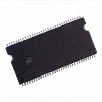
MT46V64M16P-6T:A Micron Technology Inc, MT46V64M16P-6T:A Datasheet - Page 77

MT46V64M16P-6T:A
Manufacturer Part Number
MT46V64M16P-6T:A
Description
DRAM Chip DDR SDRAM 1G-Bit 64Mx16 2.5V 66-Pin TSOP Tray
Manufacturer
Micron Technology Inc
Type
DDR SDRAMr
Datasheet
1.MT46V256M4P-6TA_TR.pdf
(82 pages)
Specifications of MT46V64M16P-6T:A
Density
1 Gb
Maximum Clock Rate
333 MHz
Package
66TSOP
Operating Supply Voltage
2.5 V
Maximum Random Access Time
0.7 ns
Operating Temperature
0 to 70 °C
Format - Memory
RAM
Memory Type
DDR SDRAM
Memory Size
1G (64M x 16)
Speed
6ns
Interface
Parallel
Voltage - Supply
2.3 V ~ 2.7 V
Package / Case
66-TSOP
Organization
64Mx16
Address Bus
16b
Access Time (max)
700ps
Operating Supply Voltage (typ)
2.5V
Package Type
TSOP
Operating Temp Range
0C to 70C
Operating Supply Voltage (max)
2.7V
Operating Supply Voltage (min)
2.3V
Supply Current
275mA
Pin Count
66
Mounting
Surface Mount
Operating Temperature Classification
Commercial
Lead Free Status / RoHS Status
Lead free / RoHS Compliant
Available stocks
Company
Part Number
Manufacturer
Quantity
Price
Company:
Part Number:
MT46V64M16P-6T:A
Manufacturer:
MICRON
Quantity:
5 530
Company:
Part Number:
MT46V64M16P-6T:A
Manufacturer:
MICRON
Quantity:
48
Part Number:
MT46V64M16P-6T:A
Manufacturer:
MICRON/美光
Quantity:
20 000
Figure 49:
PDF: 09005aef80a2f898/Source: 09005aef82a95a3a
DDR_x4x8x16_Core2.fm - 1Gb DDR: Rev. I, Core DDR: Rev. B 12/07 EN
Case 1: t AC (MIN) and t DQSCK (MIN)
Case 2: t AC (MAX) and t DQSCK (MAX)
Command
BA0, BA1
Address
DQ
DQ
DQS
DQS
CK#
CKE
A10
DM
CK
6
6
t IS
t IS
Bank READ – with Auto Precharge
NOP
T0
t IH
1
t IH
Notes:
Bank x
t IS
IS
Row
ACT
Row
T1
1. NOP commands are shown for ease of illustration; other commands may be valid at these
2. BL = 4.
3. The READ command can only be applied at T3 if
4. Enable auto precharge.
5.
6. DO n = data-out from column n; subsequent elements are provided in the programmed
7. Refer to Figure 33 on page 61, Figure 34 on page 62, and Figure 35 on page 63 for detailed
IH
t IH
t CK
times.
t
order.
DQS and DQ timing.
RP starts only after
t RAS
t RC
t RCD, t RAP 3
NOP
T2
1
t CH
t CL
READ
t IS
Bank x
4
Col n
t
RAS has been satisfied.
T3
2,3
t IH
t LZ (MIN)
CL = 2
77
NOP
T4
t RPRE
1
t LZ (MIN)
Micron Technology, Inc., reserves the right to change products or specifications without notice.
t RPRE
NOP
T5
t DQSCK (MIN)
DO
t DQSCK (MAX)
1
n
t
t AC (MIN)
DO
RAP is satisfied at T3.
t AC (MAX)
n
T5n
1Gb: x4, x8, x16 DDR SDRAM
t RP 5
NOP
T6
Transitioning Data
1
t HZ (MAX)
T6n
©2003 Micron Technology, Inc. All rights reserved.
t RPST
t RPST
NOP
T7
1
Operations
Don’t Care
Bank x
ACT
T8
Row
Row


