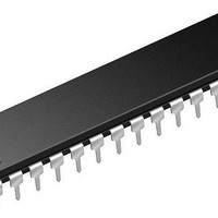
PIC16LF1518-E/SP Microchip Technology, PIC16LF1518-E/SP Datasheet - Page 112

PIC16LF1518-E/SP
Manufacturer Part Number
PIC16LF1518-E/SP
Description
28-pin, 28KB Flash, 1024B RAM, 10-bit ADC, 2xCCP, SPI, MI2C, EUSART, 1.8V-3.6V 2
Manufacturer
Microchip Technology
Series
PIC® XLP™ 16Fr
Datasheet
1.PIC16LF1517-IPT.pdf
(344 pages)
Specifications of PIC16LF1518-E/SP
Core Processor
PIC
Core Size
8-Bit
Speed
20MHz
Connectivity
I²C, LIN, SPI, UART/USART
Peripherals
Brown-out Detect/Reset, POR, PWM, WDT
Number Of I /o
25
Program Memory Size
28KB (16K x 14)
Program Memory Type
FLASH
Ram Size
1K x 8
Voltage - Supply (vcc/vdd)
1.8 V ~ 3.6 V
Data Converters
A/D 17x10b
Oscillator Type
Internal
Operating Temperature
-40°C ~ 125°C
Package / Case
*
Processor Series
PIC16LF151x
Core
PIC
Data Bus Width
8 bit
Data Ram Size
1 KB
Interface Type
I2C, SPI, USART
Maximum Clock Frequency
20 MHz
Number Of Programmable I/os
25
Number Of Timers
3
Operating Supply Voltage
1.8 V to 3.6 V
Maximum Operating Temperature
+ 125 C
Mounting Style
Through Hole
Lead Free Status / RoHS Status
Lead free / RoHS Compliant
Eeprom Size
-
Lead Free Status / Rohs Status
Details
- Current page: 112 of 344
- Download datasheet (3Mb)
PIC16(L)F1516/7/8/9
REGISTER 11-6:
TABLE 11-3:
TABLE 11-4:
DS41452A-page 112
PMCON1
PMCON2
PMADRL
PMADRH
PMDATL
PMDATH
INTCON
Legend:
CONFIG1
CONFIG2
Legend:
bit 7
Legend:
R = Readable bit
S = Bit can only be set
‘1’ = Bit is set
bit 7-0
Name
Name
W-0/0
— = unimplemented location, read as ‘0’. Shaded cells are not used by Flash Program Memory module.
— = unimplemented location, read as ‘ 0 ’. Shaded cells are not used by Flash program memory.
Bits
13:8
13:8
7:0
7:0
Bit 7
GIE
—
—
—
Flash memory Unlock Pattern bits
To unlock writes, a 55h must be written first, followed by an AAh, before setting the WR bit of the
PMCON1 register. The value written to this register is used to unlock the writes. There are specific
timing requirements on these writes.
SUMMARY OF REGISTERS ASSOCIATED WITH FLASH PROGRAM MEMORY
SUMMARY OF CONFIGURATION WORD WITH FLASH PROGRAM MEMORY
Bit -/7
W-0/0
CP
—
PMCON2: PROGRAM MEMORY CONTROL 2 REGISTER
CFGS
PEIE
Bit 6
—
MCLRE
Bit -/6
W = Writable bit
x = Bit is unknown
‘0’ = Bit is cleared
—
W-0/0
TMR0IE
LWLO
Bit 5
Program Memory Control Register 2
Bit 13/5
FCMEN
PWRTE
Program Memory Control Register 2
LVP
—
W-0/0
FREE
INTE
Bit 4
Preliminary
PMADRL<7:0>
PMDATL<7:0>
VCAPEN
Bit 12/4
DEBUG
IESO
PMADRH<6:0>
WDTE<1:0>
(1)
U = Unimplemented bit, read as ‘0’
-n/n = Value at POR and BOR/Value at all other Resets
WRERR
IOCIE
Bit 3
W-0/0
PMDATH<5:0>
CLKOUTEN
Bit 11/3
—
—
TMR0IF
WREN
Bit 2
Bit 10/2
BORV
W-0/0
—
BOREN<1:0>
Bit 1
INTF
WR
FOSC<2:0>
STVREN
2010 Microchip Technology Inc.
Bit 9/1
WRT<1:0>
W-0/0
IOCIF
Bit 0
RD
Bit 8/0
—
—
Register on
W-0/0
Page
Register
on Page
111
112
110
110
110
110
80
46
48
bit 0
Related parts for PIC16LF1518-E/SP
Image
Part Number
Description
Manufacturer
Datasheet
Request
R

Part Number:
Description:
IC, 8BIT MCU, PIC16LF, 32MHZ, QFN-28
Manufacturer:
Microchip Technology
Datasheet:

Part Number:
Description:
IC, 8BIT MCU, PIC16LF, 32MHZ, QFN-28
Manufacturer:
Microchip Technology
Datasheet:

Part Number:
Description:
IC, 8BIT MCU, PIC16LF, 32MHZ, DIP-18
Manufacturer:
Microchip Technology
Datasheet:

Part Number:
Description:
IC, 8BIT MCU, PIC16LF, 20MHZ, TQFP-44
Manufacturer:
Microchip Technology
Datasheet:

Part Number:
Description:
7 KB Flash, 384 Bytes RAM, 32 MHz Int. Osc, 16 I/0, Enhanced Mid Range Core, Nan
Manufacturer:
Microchip Technology

Part Number:
Description:
14KB Flash, 512B RAM, LCD, 11x10b ADC, EUSART, NanoWatt XLP 28 SOIC .300in T/R
Manufacturer:
Microchip Technology
Datasheet:

Part Number:
Description:
14KB Flash, 512B RAM, LCD, 11x10b ADC, EUSART, NanoWatt XLP 28 SSOP .209in T/R
Manufacturer:
Microchip Technology
Datasheet:

Part Number:
Description:
MCU PIC 14KB FLASH XLP 28-SSOP
Manufacturer:
Microchip Technology

Part Number:
Description:
MCU PIC 14KB FLASH XLP 28-SOIC
Manufacturer:
Microchip Technology

Part Number:
Description:
MCU PIC 512B FLASH XLP 28-UQFN
Manufacturer:
Microchip Technology

Part Number:
Description:
MCU PIC 14KB FLASH XLP 28-SPDIP
Manufacturer:
Microchip Technology

Part Number:
Description:
MCU 7KB FLASH 256B RAM 40-UQFN
Manufacturer:
Microchip Technology

Part Number:
Description:
MCU 7KB FLASH 256B RAM 44-TQFP
Manufacturer:
Microchip Technology

Part Number:
Description:
MCU 14KB FLASH 1KB RAM 28-UQFN
Manufacturer:
Microchip Technology

Part Number:
Description:
MCU PIC 14KB FLASH XLP 40-UQFN
Manufacturer:
Microchip Technology


