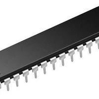
PIC16LF1518-E/SP Microchip Technology, PIC16LF1518-E/SP Datasheet - Page 113

PIC16LF1518-E/SP
Manufacturer Part Number
PIC16LF1518-E/SP
Description
28-pin, 28KB Flash, 1024B RAM, 10-bit ADC, 2xCCP, SPI, MI2C, EUSART, 1.8V-3.6V 2
Manufacturer
Microchip Technology
Series
PIC® XLP™ 16Fr
Datasheet
1.PIC16LF1517-IPT.pdf
(344 pages)
Specifications of PIC16LF1518-E/SP
Core Processor
PIC
Core Size
8-Bit
Speed
20MHz
Connectivity
I²C, LIN, SPI, UART/USART
Peripherals
Brown-out Detect/Reset, POR, PWM, WDT
Number Of I /o
25
Program Memory Size
28KB (16K x 14)
Program Memory Type
FLASH
Ram Size
1K x 8
Voltage - Supply (vcc/vdd)
1.8 V ~ 3.6 V
Data Converters
A/D 17x10b
Oscillator Type
Internal
Operating Temperature
-40°C ~ 125°C
Package / Case
*
Processor Series
PIC16LF151x
Core
PIC
Data Bus Width
8 bit
Data Ram Size
1 KB
Interface Type
I2C, SPI, USART
Maximum Clock Frequency
20 MHz
Number Of Programmable I/os
25
Number Of Timers
3
Operating Supply Voltage
1.8 V to 3.6 V
Maximum Operating Temperature
+ 125 C
Mounting Style
Through Hole
Lead Free Status / RoHS Status
Lead free / RoHS Compliant
Eeprom Size
-
Lead Free Status / Rohs Status
Details
- Current page: 113 of 344
- Download datasheet (3Mb)
12.0
In general, when a peripheral is enabled, that pin may
not be used as a general purpose I/O pin.
Each port has three standard registers for its operation.
These registers are:
• TRISx registers (data direction)
• PORTx registers (reads the levels on the pins of
• LATx registers (output latch)
Some ports may have one or more of the following
additional registers. These registers are:
• ANSELx (analog select)
• WPUx (weak pull-up)
TABLE 12-1:
The Data Latch (LATx register) is useful for
read-modify-write operations on the value that the I/O
pins are driving.
A write operation to the LATx register has the same
affect as a write to the corresponding PORTx register.
A read of the LATx register reads of the values held in
the I/O PORT latches, while a read of the PORTx
register reads the actual I/O pin value.
The port has analog functions and has an ANSELx
register which can disable the digital input and save
power. A simplified model of a generic I/O port, without
the interfaces to other peripherals, is shown in
Figure
2010 Microchip Technology Inc.
Device
PIC16(L)F1516/8
PIC16(L)F1517/9
the device)
12-1.
I/O PORTS
PORT AVAILABILITY PER
DEVICE
●
●
●
●
●
●
●
●
●
Preliminary
FIGURE 12-1:
To peripherals
Write PORTx
Write LATx
Data Bus
PIC16(L)F1516/7/8/9
Read PORTx
Data Register
D
CK
Read LATx
ANSELx
GENERIC I/O PORT
OPERATION
Q
TRISx
DS41452A-page 113
V
V
DD
SS
I/O pin
Related parts for PIC16LF1518-E/SP
Image
Part Number
Description
Manufacturer
Datasheet
Request
R

Part Number:
Description:
IC, 8BIT MCU, PIC16LF, 32MHZ, QFN-28
Manufacturer:
Microchip Technology
Datasheet:

Part Number:
Description:
IC, 8BIT MCU, PIC16LF, 32MHZ, QFN-28
Manufacturer:
Microchip Technology
Datasheet:

Part Number:
Description:
IC, 8BIT MCU, PIC16LF, 32MHZ, DIP-18
Manufacturer:
Microchip Technology
Datasheet:

Part Number:
Description:
IC, 8BIT MCU, PIC16LF, 20MHZ, TQFP-44
Manufacturer:
Microchip Technology
Datasheet:

Part Number:
Description:
7 KB Flash, 384 Bytes RAM, 32 MHz Int. Osc, 16 I/0, Enhanced Mid Range Core, Nan
Manufacturer:
Microchip Technology

Part Number:
Description:
14KB Flash, 512B RAM, LCD, 11x10b ADC, EUSART, NanoWatt XLP 28 SOIC .300in T/R
Manufacturer:
Microchip Technology
Datasheet:

Part Number:
Description:
14KB Flash, 512B RAM, LCD, 11x10b ADC, EUSART, NanoWatt XLP 28 SSOP .209in T/R
Manufacturer:
Microchip Technology
Datasheet:

Part Number:
Description:
MCU PIC 14KB FLASH XLP 28-SSOP
Manufacturer:
Microchip Technology

Part Number:
Description:
MCU PIC 14KB FLASH XLP 28-SOIC
Manufacturer:
Microchip Technology

Part Number:
Description:
MCU PIC 512B FLASH XLP 28-UQFN
Manufacturer:
Microchip Technology

Part Number:
Description:
MCU PIC 14KB FLASH XLP 28-SPDIP
Manufacturer:
Microchip Technology

Part Number:
Description:
MCU 7KB FLASH 256B RAM 40-UQFN
Manufacturer:
Microchip Technology

Part Number:
Description:
MCU 7KB FLASH 256B RAM 44-TQFP
Manufacturer:
Microchip Technology

Part Number:
Description:
MCU 14KB FLASH 1KB RAM 28-UQFN
Manufacturer:
Microchip Technology

Part Number:
Description:
MCU PIC 14KB FLASH XLP 40-UQFN
Manufacturer:
Microchip Technology


