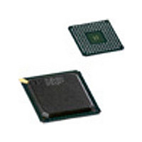
SAA7118E NXP Semiconductors, SAA7118E Datasheet - Page 78

SAA7118E
Manufacturer Part Number
SAA7118E
Description
Manufacturer
NXP Semiconductors
Datasheet
1.SAA7118E.pdf
(177 pages)
Specifications of SAA7118E
Adc/dac Resolution
9b
Screening Level
Commercial
Package Type
LBGA
Pin Count
156
Lead Free Status / RoHS Status
Compliant
Available stocks
Company
Part Number
Manufacturer
Quantity
Price
Part Number:
SAA7118E
Manufacturer:
PHILIPS/飞利浦
Quantity:
20 000
Company:
Part Number:
SAA7118E-V1
Manufacturer:
NXP
Quantity:
5 510
Company:
Part Number:
SAA7118E-V1
Manufacturer:
AD
Quantity:
5 510
Company:
Part Number:
SAA7118E/V1
Manufacturer:
PHI
Quantity:
480
Part Number:
SAA7118E/V1
Manufacturer:
PHILIPS/飞利浦
Quantity:
20 000
Company:
Part Number:
SAA7118E/V1,518
Manufacturer:
NXP Semiconductors
Quantity:
10 000
Company:
Part Number:
SAA7118E/V1,551
Manufacturer:
NXP Semiconductors
Quantity:
10 000
Company:
Part Number:
SAA7118E/V1,557
Manufacturer:
NXP Semiconductors
Quantity:
10 000
Part Number:
SAA7118E/V1/M5
Manufacturer:
PHILIPS/飞利浦
Quantity:
20 000
Company:
Part Number:
SAA7118E/V1/M5,518
Manufacturer:
Sigma Designs Inc
Quantity:
10 000
Company:
Part Number:
SAA7118EH
Manufacturer:
MNDSPEED
Quantity:
335
NXP Semiconductors
SAA7118_7
Product data sheet
The data formats at the image port are defined in double words of 32 bits (4 bytes), such
as the related FIFO structures. However the physical data stream at the image port is only
16-bit or 8-bit wide; in 16-bit mode data pins HPD7 to HPD0 are used for chrominance
data. The four bytes of the double words are serialized in words or bytes.
Available formats are as follows:
For handshake with the receiving VGA controller, or other memory or bus interface
circuitry, F, H and V reference signals and programmable FIFO flags are provided. The
information is provided on pins IGP0, IGP1, IGPH and IGPV. The functionality on these
pins is controlled via subaddresses 84h and 85h.
VBI data is collected over an entire line in its own FIFO, and transferred as an
uninterrupted block of bytes. Decoded VBI data can be signed by the VBI flag on pin IGP0
or IGP1.
As scaled video data and decoded VBI data may come from different and asynchronous
sources, an arbitration scheme is needed. Normally the VBI data slicer has priority.
The image port consists of the pins and/or signals, as listed in
For pin constrained applications, or interfaces, the relevant timing and data reference
signals can also get encoded into the data stream. Therefore the corresponding pins do
not need to be connected. The minimum image port configuration requires 9 pins only, i.e.
8 pins for data including codes, and 1 pin for clock or gated clock. The inserted codes are
defined in close relationship to the ITU-R BT.656 (D1) recommendation, where possible.
The following deviations from “ITU 656 recommendation” are implemented at the
SAA7118 image port interface:
•
•
•
•
•
•
•
•
•
•
•
Y-C
Y-C
Raw samples
Decoded VBI data
SAV and EAV codes are only present in those lines, where data is to be transferred,
i.e. active video lines, or VBI raw samples, no codes for empty lines
There may be more or less than 720 pixels between SAV and EAV
Data content and the number of clock cycles during horizontal and vertical blanking is
undefined, and may not be constant
Data stream may be interleaved with not-valid data codes, 00h, but SAV and EAV
4-byte codes are not interleaved with not-valid data codes
There may be an irregular pattern of not-valid data, or IDQ, and as a result, C
is not in a fixed phase to a regular clock divider
VBI raw sample streams are enveloped with SAV and EAV, like normal video
Decoded VBI data is transported as Ancillary (ANC) data, two modes:
– Direct decoded VBI data bytes (8-bit) are directly placed in the ANC data field,
00h and FFh codes may appear in data block (violation to ITU-R BT.656)
B
B
-C
-C
R
R
4 : 2 : 2
4 : 1 : 1
Rev. 07 — 7 July 2008
Multistandard video decoder with adaptive comb filter
Table
33.
SAA7118
© NXP B.V. 2008. All rights reserved.
B
-Y-C
78 of 177
R
-Y


