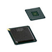
SAA7105E/V1/G.557 NXP Semiconductors, SAA7105E/V1/G.557 Datasheet - Page 41

SAA7105E/V1/G.557
Manufacturer Part Number
SAA7105E/V1/G.557
Description
Manufacturer
NXP Semiconductors
Datasheet
1.SAA7105EV1G.557.pdf
(78 pages)
Specifications of SAA7105E/V1/G.557
Adc/dac Resolution
10b
Screening Level
Commercial
Package Type
LBGA
Pin Count
156
Lead Free Status / RoHS Status
Compliant
- Current page: 41 of 78
- Download datasheet (359Kb)
Philips Semiconductors
SAA7104E_SAA7105E_2
Product data sheet
Table 39:
Table 40:
Legend: * = default value after reset.
Bit
7 and 6 CCRS[1:0]
5 to 0
Bit
7
6
5
4
3
2
1
0
Symbol
BLNVB[5:0] R/W
Symbol
DOWND
DOWNA
INPI
YGS
-
SCBW
PAL
FISE
CCR and blanking level VBI register, subaddress 5Fh, bit description
Standard control register, subaddress 61h, bit description
Rev. 02 — 23 December 2005
Access Value Description
R/W
Access Value Description
R/W
R/W
R/W
R/W
R/W
R/W
R/W
R/W
00
01
10
11
-
0*
1
0*
1
0*
1
0
1
0
0
1*
0
1
0
1
select cross-color reduction filter in luminance; for overall
transfer characteristic of luminance see
no cross-color reduction
cross-color reduction #1 active
cross-color reduction #2 active
cross-color reduction #3 active
variable blanking level during vertical blanking interval is
typically identical to value of BLNNL
digital core
in normal operational mode
in Sleep mode and is reactivated with an I
DACs
in normal operational mode
in Power-down mode
PAL switch
phase is nominal
is inverted compared to nominal if RTCE = 1
luminance gain for white
100 IRE
92.5 IRE including 7.5 IRE set-up of black
must be programmed with logic 0 to ensure compatibility
to future enhancements
bandwidth for chrominance encoding (for overall transfer
characteristic of chrominance in baseband representation
see
enlarged
standard
encoding
NTSC (non-alternating V component)
PAL (alternating V component)
total pixel clocks per line
864
858
Figure 6
SAA7104E; SAA7105E
and
Figure
© Koninklijke Philips Electronics N.V. 2005. All rights reserved.
7)
black
Digital video encoder
Figure 8
2
C-bus address
41 of 78
Related parts for SAA7105E/V1/G.557
Image
Part Number
Description
Manufacturer
Datasheet
Request
R
Part Number:
Description:
IC DIGITAL VIDEO ENCODER 156LBGA
Manufacturer:
NXP Semiconductors
Datasheet:
Part Number:
Description:
IC DIGITAL VIDEO ENCODER 156LBGA
Manufacturer:
NXP Semiconductors
Datasheet:
Part Number:
Description:
IC DIGITAL VIDEO ENCODER 156LBGA
Manufacturer:
NXP Semiconductors
Datasheet:
Part Number:
Description:
IC DIGITAL VIDEO ENCODER 156LBGA
Manufacturer:
NXP Semiconductors
Datasheet:
Part Number:
Description:
Video ICs PC-DENC
Manufacturer:
NXP Semiconductors
Datasheet:
Part Number:
Description:
Video ICs PC-DENC
Manufacturer:
NXP Semiconductors
Datasheet:
Part Number:
Description:
Digital Video Encoder
Manufacturer:
NXP Semiconductors
Datasheet:
Part Number:
Description:
Digital Video Encoder
Manufacturer:
NXP Semiconductors
Datasheet:
Part Number:
Description:
NXP Semiconductors designed the LPC2420/2460 microcontroller around a 16-bit/32-bitARM7TDMI-S CPU core with real-time debug interfaces that include both JTAG andembedded trace
Manufacturer:
NXP Semiconductors
Datasheet:

Part Number:
Description:
NXP Semiconductors designed the LPC2458 microcontroller around a 16-bit/32-bitARM7TDMI-S CPU core with real-time debug interfaces that include both JTAG andembedded trace
Manufacturer:
NXP Semiconductors
Datasheet:
Part Number:
Description:
NXP Semiconductors designed the LPC2468 microcontroller around a 16-bit/32-bitARM7TDMI-S CPU core with real-time debug interfaces that include both JTAG andembedded trace
Manufacturer:
NXP Semiconductors
Datasheet:
Part Number:
Description:
NXP Semiconductors designed the LPC2470 microcontroller, powered by theARM7TDMI-S core, to be a highly integrated microcontroller for a wide range ofapplications that require advanced communications and high quality graphic displays
Manufacturer:
NXP Semiconductors
Datasheet:
Part Number:
Description:
NXP Semiconductors designed the LPC2478 microcontroller, powered by theARM7TDMI-S core, to be a highly integrated microcontroller for a wide range ofapplications that require advanced communications and high quality graphic displays
Manufacturer:
NXP Semiconductors
Datasheet:
Part Number:
Description:
The Philips Semiconductors XA (eXtended Architecture) family of 16-bit single-chip microcontrollers is powerful enough to easily handle the requirements of high performance embedded applications, yet inexpensive enough to compete in the market for hi
Manufacturer:
NXP Semiconductors
Datasheet:


