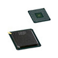
SAA7105E/V1/G.557 NXP Semiconductors, SAA7105E/V1/G.557 Datasheet - Page 63

SAA7105E/V1/G.557
Manufacturer Part Number
SAA7105E/V1/G.557
Description
Manufacturer
NXP Semiconductors
Datasheet
1.SAA7105EV1G.557.pdf
(78 pages)
Specifications of SAA7105E/V1/G.557
Adc/dac Resolution
10b
Screening Level
Commercial
Package Type
LBGA
Pin Count
156
Lead Free Status / RoHS Status
Compliant
- Current page: 63 of 78
- Download datasheet (359Kb)
Philips Semiconductors
Table 112: Characteristics
T
SAA7104E_SAA7105E_2
Product data sheet
Symbol
Outputs
V
V
I
V
V
I
V
I
Clock timing; pins PIXCLKI and PIXCLKO
T
t
t
t
Input timing
t
t
Crystal oscillator
f
Crystal specification
T
C
R
C
C
2
i
o
d(CLKD)
r
f
SU;DAT
HD;DAT
nom
amb
PIXCLK
f/f
amb
OL
OH
C-bus; pins SDA and SCL
IL
IH
OL
L
S
1
0
nom
= 0 C to 70 C (typical values excluded); unless otherwise specified.
Parameter
LOW-level output
voltage
HIGH-level output
voltage
LOW-level input voltage
HIGH-level input voltage
input current
LOW-level output
voltage (pin SDA)
output current
cycle time
delay from PIXCLKO to
PIXCLKI
duty factor
rise time
fall time
input data set-up time
input data hold time
nominal frequency
permissible deviation of
nominal frequency
ambient temperature
load capacitance
series resistance
motional capacitance
(typical)
parallel capacitance
(typical)
…continued
Conditions
V
V
pins TDO, TTXRQ_XCLKO2, VSM
and HSM_CSYNC
V
V
pins TDO, TTXRQ_XCLKO2, VSM
and HSM_CSYNC
V
I
during acknowledge
t
t
pins PD11 to PD0
pins HSVGC, VSVGC and FSVGC
pins PD11 to PD0
pins HSVGC, VSVGC and FSVGC
OL
HIGH
HIGH
DDD1
DDD1
DDD1
DDD1
i
= LOW or HIGH
= 3 mA
/T
/T
= 1.1 V, 1.5 V, 1.8 V or 2.5 V
= 3.3 V
= 1.1 V, 1.5 V, 1.8 V or 2.5 V
= 3.3 V
PIXCLK
CLKO2
Rev. 02 — 23 December 2005
; output
SAA7104E; SAA7105E
[3]
[3]
[3]
[3]
[4]
[5]
[4]
[4]
[4]
[6]
[6]
[7]
Min
0
0
0
V
2.4
2.4
0.7V
-
3
12
-
40
40
-
-
2
2
0.9
1.5
-
0
8
-
1.2
2.8
0.5
10
50
DDD1
DDD2
10
© Koninklijke Philips Electronics N.V. 2005. All rights reserved.
0.1 -
6
Typ
-
-
-
-
-
-
-
-
-
-
-
-
50
50
-
-
-
-
-
-
27
-
-
-
-
1.5
3.5
Digital video encoder
Max
0.1
0.4
0.4
V
V
V
0.3V
V
+10
0.4
-
-
-
60
60
1.5
1.5
-
-
-
-
-
+50
70
-
80
1.8
4.2
DDD1
DDD1
DDD2
DDD2
DDD2
10
+ 0.3
6
63 of 78
Unit
V
V
V
V
V
V
V
V
V
mA
ns
ns
%
%
ns
ns
ns
ns
ns
ns
MHz
pF
fF
pF
C
A
Related parts for SAA7105E/V1/G.557
Image
Part Number
Description
Manufacturer
Datasheet
Request
R
Part Number:
Description:
IC DIGITAL VIDEO ENCODER 156LBGA
Manufacturer:
NXP Semiconductors
Datasheet:
Part Number:
Description:
IC DIGITAL VIDEO ENCODER 156LBGA
Manufacturer:
NXP Semiconductors
Datasheet:
Part Number:
Description:
IC DIGITAL VIDEO ENCODER 156LBGA
Manufacturer:
NXP Semiconductors
Datasheet:
Part Number:
Description:
IC DIGITAL VIDEO ENCODER 156LBGA
Manufacturer:
NXP Semiconductors
Datasheet:
Part Number:
Description:
Video ICs PC-DENC
Manufacturer:
NXP Semiconductors
Datasheet:
Part Number:
Description:
Video ICs PC-DENC
Manufacturer:
NXP Semiconductors
Datasheet:
Part Number:
Description:
Digital Video Encoder
Manufacturer:
NXP Semiconductors
Datasheet:
Part Number:
Description:
Digital Video Encoder
Manufacturer:
NXP Semiconductors
Datasheet:
Part Number:
Description:
NXP Semiconductors designed the LPC2420/2460 microcontroller around a 16-bit/32-bitARM7TDMI-S CPU core with real-time debug interfaces that include both JTAG andembedded trace
Manufacturer:
NXP Semiconductors
Datasheet:

Part Number:
Description:
NXP Semiconductors designed the LPC2458 microcontroller around a 16-bit/32-bitARM7TDMI-S CPU core with real-time debug interfaces that include both JTAG andembedded trace
Manufacturer:
NXP Semiconductors
Datasheet:
Part Number:
Description:
NXP Semiconductors designed the LPC2468 microcontroller around a 16-bit/32-bitARM7TDMI-S CPU core with real-time debug interfaces that include both JTAG andembedded trace
Manufacturer:
NXP Semiconductors
Datasheet:
Part Number:
Description:
NXP Semiconductors designed the LPC2470 microcontroller, powered by theARM7TDMI-S core, to be a highly integrated microcontroller for a wide range ofapplications that require advanced communications and high quality graphic displays
Manufacturer:
NXP Semiconductors
Datasheet:
Part Number:
Description:
NXP Semiconductors designed the LPC2478 microcontroller, powered by theARM7TDMI-S core, to be a highly integrated microcontroller for a wide range ofapplications that require advanced communications and high quality graphic displays
Manufacturer:
NXP Semiconductors
Datasheet:
Part Number:
Description:
The Philips Semiconductors XA (eXtended Architecture) family of 16-bit single-chip microcontrollers is powerful enough to easily handle the requirements of high performance embedded applications, yet inexpensive enough to compete in the market for hi
Manufacturer:
NXP Semiconductors
Datasheet:


