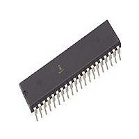
CP82C37A-5 Intersil, CP82C37A-5 Datasheet

CP82C37A-5
Specifications of CP82C37A-5
Available stocks
Related parts for CP82C37A-5
CP82C37A-5 Summary of contents
Page 1
... Each channel has a full 64K address and word count range, and may be programmed to autoinitialize these registers following DMA termination (end of process). Ordering Information PART 5MHz MARKING 8MHz CP82C37A-5 CP82C37A-5 CP82C37A IP82C37A-5 IP82C37A CS82C37A-5 CS82C37A* CS82C37AZ (Note) CS82C37AZ IS82C37A-5 IS82C37A CD82C37A-5 ...
Page 2
Pinouts 82C37A (PDIP/CERDIP) TOP VIEW IOR 1 IOW 2 MEMR 3 MEMW READY 6 HLDA 7 ADSTB 8 AEN 9 HRQ CLK 12 RESET 13 DACK2 14 DACK3 15 DREQ3 16 DREQ2 17 DREQ1 ...
Page 3
Pin Description PIN SYMBOL NUMBER TYPE decoupling. GND 20 Ground CLK 12 I CLOCK INPUT: The Clock Input is used to generate the timing signals which control 82C37A operations. This input may be driven from ...
Page 4
Pin Description (Continued) PIN SYMBOL NUMBER TYPE EOP 36 I/O END OF PROCESS: End of Process (EOP active low bidirectional signal. Information concerning the completion of DMA services is available at the bidirectional EOP pin. The 82C37A allows ...
Page 5
Functional Description The 82C37A direct memory access controller is designed to improve the data transfer rate in systems which must transfer data from an I/O device to memory, or move a block of memory to an I/O device. It will ...
Page 6
The active cycle is composed of several internal states, depending on what options have been selected and what type of operation has been requested. The 82C37A can assume seven separate states, each composed ...
Page 7
After the I/O device has had a chance to catch up, the DMA service is reestablished by means of a DREQ. During the time between services when the microprocessor is allowed to operate, the intermediate values of address and word ...
Page 8
Channel 0 word count decrementing to FFFFH will not set the channel 0 TC bit in the status register nor generate an EOP, nor set the channel 0 mask bit in this mode. It will cause an autoinitialization of channel ...
Page 9
Programming The 82C37A will accept programming from the host processor anytime that HLDA is inactive, and at least one rising clock edge has occurred after HLDA went low the responsibility of the host to assure that programming and ...
Page 10
See the following diagram and Figure 4 for Mode register functions and addresses. Mode Register BIT NUMBER 00 Channel 0 select 01 Channel 1 select 10 Channel 2 select ...
Page 11
Status Bits 4-7 are cleared upon RESET or Master Clear. Status Register BIT NUMBER 1 Channel 0 has reached TC 1 Channel 1 has reached TC 1 Channel 2 has reached ...
Page 12
External EOP Operation The EOP pin is a bidirectional, open drain pin which may be driven by external signals to terminate DMA operation. Because EOP is an open drain pin an external pull-up resistor required. The value ...
Page 13
DMA controller to accomplish the DMA transfers. Data is transferred directly from the I/O device to memory (or vice versa) with IOR and MEMW (or MEMR and IOW) being HLDA 82C84A ...
Page 14
Figure 7 shows an application for a DMA system using the 82C37A DMA controller and the 80C286 Microprocessor. In this application, the system clock comes from the 82C284 clock generator PCLK signal which is inverted to provide proper READY setup ...
Page 15
Absolute Maximum Ratings Supply Voltage . . . . . . . . . . . . . . . . . . . . . . . . . . . . . . . . . . . ...
Page 16
AC Electrical Specifications SYMBOL PARAMETER DMA (MASTER) MODE (1)TAEL AEN HIGH from CLK LOW (S1) Delay Time (2)TAET AEN LOW from CLK HIGH (SI) Delay Time (3)TAFAB ADR Active to Float Delay from CLK HIGH ...
Page 17
AC Electrical Specifications SYMBOL PARAMETER (21)TEPW EOP Pulse Width (22)TFAAB ADR Valid Delay from CLK HIGH (23)TFAC READ or WRITE Active from CLK HIGH (24)TFADB DB Valid Delay from CLK HIGH (25)THS HLDA Valid to CLK HIGH ...
Page 18
AC Electrical Specifications SYMBOL PARAMETER (62)TDVWL DACK Valid to WRITE LOW (63)TRHDI READ HIGH to DACK Inactive (64)TAZRL ADR Float to READ LOW PERIPHERAL (SLAVE) MODE (41)TAR ADR Valid or CS LOW to READ LOW (42)TAWL ADR ...
Page 19
Timing Waveforms CS IOW TAWL DB0 - DB7 NOTE: Successive WRITE accesses to the 82C37A must allow at least TCY as recovery time between accesses. A TCY recovery time must be allowed before executing a WRITE access ...
Page 20
Timing Waveforms (Continued CLK TQS (30) DREQ TDQ (18) HRQ THS (25) HLDA AEN ADSTB DB0-DB7 A0-A7 DACK READ WRITE (FOR EXTENDED WRITE) INT EOP EXT EOP 20 82C37A 82C37A TAEL ...
Page 21
Timing Waveforms (Continued) S0 S11 CLK (33) TCLSL TCLSH ADSTB TFAAB (22) TASS (11) A0-A7 TFADB (24) DB0-DB7 TDCL (15) TFAC (23) MEMR TFAC (23) MEMW EOP EXT EOP S2 CLK READ WRITE EXTENDED WRITE READY NOTE: READY must not ...
Page 22
Timing Waveforms (Continued) CLK A0-A7 READ WRITE READY RESET IOR OR IOW AC Test Circuits V1 R1 OUTPUT FROM DEVICE UNDER TEST C1 (NOTE) NOTE: Includes STRAY and FIXTURE Capacitance TEST CONDITION DEFINITION TABLE PINS V1 All Outputs Except EOP ...
Page 23
Burn-In Circuits VCC/2 VCC/2 VCC/2 VCC/2 VCC/2 VCC/2 VCC/2 VCC/2 GND OPEN OPEN DO5 VCC/2 VCC/2 VCC/2 DO5 F1 D06 VCC/2 OPEN NOTES: = 5.5V ± 0. VIH = 4.5V ± 10% 3. VIL = -0.2V ...
Page 24
... Accordingly, the reader is cautioned to verify that data sheets are current before placing orders. Information furnished by Intersil is believed to be accurate and reliable. However, no responsibility is assumed by Intersil or its subsidiaries for its use; nor for any infringements of patents or other rights of third parties which may result from its use ...


