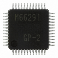
M66291GP#201 Renesas Electronics America, M66291GP#201 Datasheet - Page 13

M66291GP#201
Manufacturer Part Number
M66291GP#201
Description
IC USB CONTROLLER GEN-PUR 48LQFP
Manufacturer
Renesas Electronics America
Datasheet
1.M66291GP201.pdf
(126 pages)
Specifications of M66291GP#201
Package / Case
48-LQFP
Mounting Type
Surface Mount
Current - Supply
30mA
Voltage - Supply
3 V ~ 3.6 V
Operating Temperature
-20°C ~ 85°C
Interface
Serial
Controller Type
USB 2.0 Controller
Lead Free Status / RoHS Status
Not Compliant
Available stocks
Company
Part Number
Manufacturer
Quantity
Price
M 6 6 2 9 1 G P / H P
R e v 1 . 0 1
(3) Xtal (Clock Select) Bits (b13~b12)
(4) SCKE (Internal Clock Enable) Bit (b11)
(5) USBPC (USB Transceiver Power Control) Bit (b10)
(6) Tr_on (Tr_on Output Control) Bits (b9~b8)
(7) USBE (USB Module Operation Enable) Bit (b0)
These bits set the multiplication factor of the external clock into PLL.
Since it is necessary to supply 48 MHz to the core block, the setting values of these bits are determined by the
clock frequency to be input into the PLL.
Refer to Figure 2.3.
This bit sets the clock supply into the core block.
Set the PLLC bit to “1” and wait until the oscillation of the PLL stabilizes before setting this bit to “1”.
Refer to Figure 2.3.
This bit sets the enable/disable of the USB transceiver block of I/O block.
Even if this bit is set to “0”, it is possible to receive the resume signal during the Suspended state (DVSQ bits
= “1xx”). It is necessary that the Tr_on bits be set to “x1” (during operation of SIE block).
These bits set the TrON signal output from I/O block and the enable/disable of SIE block in core block.
This bit sets S/W reset.
When this bit is set to “0”, the M66291 enters the S/W reset state and the registers are set to their S/W reset
state.
.
2 0 0 4 . 1 1 . 0 1
External clock
p a g e 1 3 o f 1 2 2
O scillation
XCKE bit
Figure 2.3 Clock Control
buffer
Enable/Disable
I/O block
PLLC bit
Xtal bits
PLL
Enable/Disable
Multiplying
factor
Core block
SCKE bit


