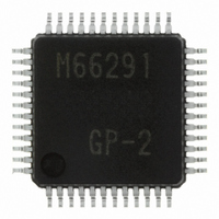
M66291GP#201 Renesas Electronics America, M66291GP#201 Datasheet - Page 65

M66291GP#201
Manufacturer Part Number
M66291GP#201
Description
IC USB CONTROLLER GEN-PUR 48LQFP
Manufacturer
Renesas Electronics America
Datasheet
1.M66291GP201.pdf
(126 pages)
Specifications of M66291GP#201
Package / Case
48-LQFP
Mounting Type
Surface Mount
Current - Supply
30mA
Voltage - Supply
3 V ~ 3.6 V
Operating Temperature
-20°C ~ 85°C
Interface
Serial
Controller Type
USB 2.0 Controller
Lead Free Status / RoHS Status
Not Compliant
Available stocks
Company
Part Number
Manufacturer
Quantity
Price
M 6 6 2 9 1 G P / H P
R e v 1 . 0 1
(6) INTM (DMA Interrupt Mode) Bit (b9)
(7) DMAEN (DMA Enable) Bit (b8)
(8) BSWP (Byte Swap Mode) Bit (b7)
This bit sets the timing of setting “1” to the EPB_RDY bit.
<When set to OUT buffer (EPi_DIR bit = “0”)>
<When set to IN buffer (EPi_DIR bit = “1”)>
This bit sets the enable/disable of the output of the DREQ signal for DMA transfer.
When this bit is set to “1”, the DMA transfer is set to enable mode, making the DREQ signal ready for
assertion.
When this bit is written to “0”, the DMA transfer is disabled, allowing no output of DREQ signal.
This bit sets the endian of the Dn_FIFO Data Register.
When this bit is set to “0”, the Dn_FIFO Data Register gets such as little endian.
When this bit is set to “1”, the Dn_FIFO Data Register gets such as big endian.
2 0 0 4 . 1 1 . 0 1
Note:
Note:
Note:
When this bit is set to “0”, the EPB_RDY bit is set to “1” after reading all buffer data including the
received short packet (including the zero-length packet) <buffer ready interrupt occurs>.
In case of reading the buffer, the buffer state as well as the bits below are retained. This enables the
reading of the received data length using the buffer ready interrupt.
It is necessary to write “1” to the BCLR bit and to clean the buffer in order to receive the next data.
Thus clears the IVAL bit to “0”, and the EPB_RDY bits also are cleared if the RDYM bit is set to “0”. If
the RDYM bit is set to “1”, the EPB_RDY bits are cleared to “0” by writing “0” to the EPB_RDY bit.
When this bit is set to “1”, the EPB_RDY bit is set to “1” under the same conditions as the endpoint not
specified by the DMA_EP bits (buffer ready interrupt occurs).
When this bit is set to “0”, the EPB_RDY bit cannot be set to “1”.
When this bit is set to “1”, the EPB_RDY bit is set to “1” under the same conditions as the endpoint not
specified by the DMA_EP bits (buffer ready interrupt occurs).
Do not use with DMAEN = “0” when this bit is set to “0”.
Do not use with INTM = “0” when this bit is set to “0”.
Don’t set this bit to “1” when the mode is set to 8-bit (set by the Octl bit or *HWR/*BYTE pin).
•
•
p a g e 6 5 o f 1 2 2
IVAL bit of the Dn_FIFO Control Register (“1” retained)
DMA_DTLN bits of the Dn_FIFO Control Register
Little Endian
Big Endian
even number address
odd number address
b15~b8
even number address
odd number address
b7~b0


