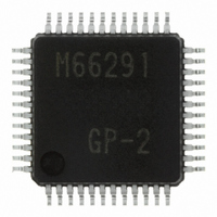
M66291GP#201 Renesas Electronics America, M66291GP#201 Datasheet - Page 88

M66291GP#201
Manufacturer Part Number
M66291GP#201
Description
IC USB CONTROLLER GEN-PUR 48LQFP
Manufacturer
Renesas Electronics America
Datasheet
1.M66291GP201.pdf
(126 pages)
Specifications of M66291GP#201
Package / Case
48-LQFP
Mounting Type
Surface Mount
Current - Supply
30mA
Voltage - Supply
3 V ~ 3.6 V
Operating Temperature
-20°C ~ 85°C
Interface
Serial
Controller Type
USB 2.0 Controller
Lead Free Status / RoHS Status
Not Compliant
Available stocks
Company
Part Number
Manufacturer
Quantity
Price
M 6 6 2 9 1 G P / H P
3.3.4
3.3.5
R e v 1 . 0 1
(1) Cycle Steal Mode (BUST bit = "0")
(2) Burst Mode (BUST bit = "1")
DMA Transfer Overview
DMA Transfer Method
The M66291 is capable of DMA transfer in 16-bit/8-bit width (specified by the Octl bit) against the endpoint 1
to 6.
The DREQ pin is asserted when the endpoint buffer set to the Dn_FIFO Select Register is in read/write ready
state. The output of DREQ pin is enabled by the DMAEN bit.
In order to write the data to transmit the short packet by the DMA_FIFO, assert the TC pin or set the IVAL
bit to “1” after writing last data.
Further, when read by using DMA, the timing of the buffer ready interrupt occurrence can be changed by the
INTM bit.
The DMA transfer method is set by the DFORM bit of the Dn_FIFO Control Register.
At cycle steal mode, the DREQ pin is asserted at every transfer (8-bit/16-bit).
At burst mode, the DREQ pin is asserted until all data in the buffer has been transferred , and is negated
when the transfer completes.
2 0 0 4 . 1 1 . 0 1
(A-1) DMA transfer control by the DACK pin and read/write pins (DFORM bits = “00”):
(A-2) DMA transfer control solely by the DACK pin (DFORM bits = “01”):
(A-3) DMA transfer control by the chip select pin and the address pins (DFORM bits = “10”):
(B-1) DMA transfer control by the DACK pin and read/write pins (DEFORM bits = “00”):
(B-2) DMA transfer control by the chip select pin and address pins (DEFORM bits = “10”):
At this mode, the DACK pin and read/write pins are used to access to the Dn_FIFO Data Register
of the M66291.
At this mode, only the DACK pin is used to access to the Dn_FIFO Data Register of the M66291.
The read/write pins are not used in this mode (are ignored).
In this mode, the address pins and read/write pins are used to access the Dn_FIFO Data Register
of the M66291. The DACK pin is not used in this mode (is ignored).
This mode operates with the same timing as (A-1).
This mode operates with the same timing as (A-3).
p a g e 8 8 o f 1 2 2


