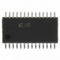
W234X Cypress Semiconductor Corp, W234X Datasheet - Page 2

W234X
Manufacturer Part Number
W234X
Description
CLOCK GEN DIR RAMBS DUAL 28TSSOP
Manufacturer
Cypress Semiconductor Corp
Type
Direct RAMbus Clock Generatorr
Datasheet
1.W234X.pdf
(14 pages)
Specifications of W234X
Input
CMOS
Output
CMOS
Frequency - Max
400MHz
Voltage - Supply
3.135 V ~ 3.465 V
Operating Temperature
0°C ~ 70°C
Mounting Type
Surface Mount
Package / Case
28-TSSOP
Frequency-max
400MHz
Lead Free Status / RoHS Status
Contains lead / RoHS non-compliant
Other names
428-1398
Available stocks
Company
Part Number
Manufacturer
Quantity
Price
Part Number:
W234X
Manufacturer:
ICW
Quantity:
20 000
Pin Definitions
Document #: 38-07232 Rev. *B
REFCLK
PCLKM0:1
SYNCLKN0:1
STOP#
PWR_DWN#
MULT 0:2
CLK0, CLK0#,
CLK1, CLK1#
S0, S1, S2
VDDIR
VDDIPD
VDD
GND
Pin Name
3, 7, 11, 21,
6, 8, 18, 25
23, 24, 20,
17, 16, 15
28, 27, 26
5, 10
4, 9
Pin
No.
13
14
19
12
22
2
1
Type
RefV
RefV
Pin
G
O
P
I
I
I
I
I
I
I
Reference Clock Input: Reference clock input, normally supplied by a system
frequency synthesizer (Cypress W133).
Phase Detector Input 0:1: The phase difference between this signal and SYN-
CLKN is used to synchronize the Rambus Channel Clock with the system clock.
Both PCLKM and SYNCLKN are provided by the Gear Ratio Logic in the memory
controller. If the Gear Ratio Logic is not used, this pin would be connected to
ground.
Phase Detector Input 0:1: The phase difference between this signal and PCLKM
is used to synchronize the Rambus Channel Clock with the system clock. Both
PCLKM and SYNCLKN are provided by the Gear Ratio Logic in the memory con-
troller. If the Gear Ratio Logic is not used, this pin would be connected to ground.
Clock Output Enable: When this input is driven to active LOW, it disables the
differential Rambus Channel clocks.
Active LOW Power-Down: When this input is driven to active LOW, it disables
the differential Rambus Channel clocks and places the W234 in Power-Down
mode.
PLL Multiplier Select: These inputs select the PLL prescaler and feedback divid-
ers to determine the multiply ratio for the PLL for the input REFCLK.
Complementary Output Clock: Differential Rambus Channel clock outputs.
Mode Control Input: These inputs control the operating mode of the W234.
Reference for Refclk: Voltage reference for input reference clock.
Reference for Phase Detector: Voltage reference for phase detector inputs and
STOP#.
Power Connection: Power supply for core logic and output buffers. Connected to
3.3V supply.
Ground Connection: Connect all ground pins to the common system ground
plane.
MULT0
0
0
0
0
1
1
1
1
S0
0
1
1
0
1
1
0
MULT1
0
0
1
1
0
0
1
1
S1
0
0
1
0
0
1
1
Pin Description
MULT2
0
1
0
1
0
1
0
1
S2
0
0
0
1
1
1
X
TBD
TBD
16
A
4
9
6
8
8
Output Test (OE)
Vendor Test A
Vendor Test B
Reserved
Normal
Bypass
MODE
Test
Page 2 of 14
TBD
TBD
B
1
2
1
3
3
1
W234


