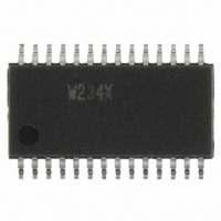
W234X Cypress Semiconductor Corp, W234X Datasheet - Page 3

W234X
Manufacturer Part Number
W234X
Description
CLOCK GEN DIR RAMBS DUAL 28TSSOP
Manufacturer
Cypress Semiconductor Corp
Type
Direct RAMbus Clock Generatorr
Datasheet
1.W234X.pdf
(14 pages)
Specifications of W234X
Input
CMOS
Output
CMOS
Frequency - Max
400MHz
Voltage - Supply
3.135 V ~ 3.465 V
Operating Temperature
0°C ~ 70°C
Mounting Type
Surface Mount
Package / Case
28-TSSOP
Frequency-max
400MHz
Lead Free Status / RoHS Status
Contains lead / RoHS non-compliant
Other names
428-1398
Available stocks
Company
Part Number
Manufacturer
Quantity
Price
Part Number:
W234X
Manufacturer:
ICW
Quantity:
20 000
DDLL System Architecture and Gear Ratio Logic
Figure 1 shows the Distributed Delay Lock Loop (DDLL) sys-
tem architecture, including the main system clock source, the
Direct Rambus clock generator (DRCG), and the core logic
that contains the Rambus Access Cell (RAC), the Rambus
Memory Controller (RMC), and the Gear Ratio Logic. (This
diagram abstractly represents the differential clocks as a sin-
gle Busclk wire.)
The purpose of the DDLL is to frequency-lock and phase-align
the core logic and Rambus clocks (PCLK and SYNCLK) at the
RMC/RAC boundary in order to allow data transfers without
incurring additional latency. In the DDLL architecture, a PLL is
used to generate the desired Busclk frequency, while a distrib-
uted loop forms a DLL to align the phase of Pclk and Synclk at
the RMC/RAC boundary.
The main clock source drives the system clock (Pclk) to the
core logic, and also drives the reference clock (Refclk) to the
DRCG. For typical Intel architecture platforms, Refclk will be
half the CPU front side bus frequency. A PLL inside the DRCG
multiplies Refclk to generate the desired frequency for Busclk,
and Busclk is driven through a terminated transmission line
(Rambus Channel). At the mid-point of the channel, the RAC
senses Busclk using its own DLL for clock alignment, followed
by a fixed divide-by-4 that generates Synclk.
Pclk is the clock used in the memory controller (RMC) in the
core logic, and Synclk is the clock used at the core logic inter-
Document #: 38-07232 Rev. *B
Synclk/N
Synclk
Pclk/M =
Pclk
CY2210-2
CY2210-3
CY2215
W133
W158
W159
W161
W167B
RMC
Pclk
Figure 1. DDLL System Architecture.
Refclk
Figure 2. Gear Ratio Timing Diagram.
W234
PLL
M
Gear
Ratio
Logic
N
Phase
Align
D
Synclk
face of the RAC. The DDLL together with the Gear Ratio Logic
enables users to exchange data directly from the Pclk domain
to the Synclk domain without incurring additional latency for
synchronization. In general, Pclk and Synclk can be of differ-
ent frequencies, so the Gear Ratio Logic must select the ap-
propriate M and N dividers such that the frequencies of Pclk/M
and Synclk/N are equal. In one interesting example,
Pclk=133 MHz, Synclk=100 MHz, and M=4 while N=3, giving
Pclk/M=Synclk/N=33 MHz. This example of the clock wave-
forms with the Gear Ratio Logic is shown in Figure 2.
The output clocks from the Gear Ratio Logic, Pclk/M, and Syn-
clk/N, are output from the core logic and routed to the DRCG
Phase Detector (
clk/N must be matched in the core logic as well as on the
board.
After comparing the phase of Pclk/M vs. Synclk/N, the DRCG
Phase Detector (
phase of the DRCG output clock, Busclk. Since everything
else in the distributed loop is fixed delay, adjusting Busclk ad-
justs the phase of Synclk and thus the phase of Synclk/N. In
this manner the distributed loop adjusts the phase of Synclk/N
to match that of Pclk/M, nulling the phase error at the input of
the DRCG Phase Detector (
data can be exchanged directly from the Pclk domain to the
Synclk domain.
4
DLL
RAC
Busclk
D
D
) inputs. The routing of Pclk/M and Syn-
) drives a phase aligner that adjusts the
D
). When the clocks are aligned,
Page 3 of 14
W234


