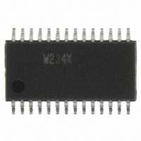
W234X Cypress Semiconductor Corp, W234X Datasheet - Page 6

W234X
Manufacturer Part Number
W234X
Description
CLOCK GEN DIR RAMBS DUAL 28TSSOP
Manufacturer
Cypress Semiconductor Corp
Type
Direct RAMbus Clock Generatorr
Datasheet
1.W234X.pdf
(14 pages)
Specifications of W234X
Input
CMOS
Output
CMOS
Frequency - Max
400MHz
Voltage - Supply
3.135 V ~ 3.465 V
Operating Temperature
0°C ~ 70°C
Mounting Type
Surface Mount
Package / Case
28-TSSOP
Frequency-max
400MHz
Lead Free Status / RoHS Status
Contains lead / RoHS non-compliant
Other names
428-1398
Available stocks
Company
Part Number
Manufacturer
Quantity
Price
Part Number:
W234X
Manufacturer:
ICW
Quantity:
20 000
In Clk Stop mode, the clock source is on, but the output is
disabled (STOP# asserted). The VDDIPD reference input may
remain on or may be grounded during the Clk Stop mode. The
VDDIR reference input must remain on during the Clk Stop
mode.
In Normal mode, the clock source is on, and the output is en-
abled.
Table 6 lists the control signals for each state.
Table 6. Control Signals for Clock Source States
Document #: 38-07232 Rev. *B
Power-Down
Clk Stop
Normal
State
PWR_DWN# STOP#
V
0
1
1
DD
Turn-On
V
DD
Test
M
Turn-On
X
0
1
K
Power-Down
Source
Figure 4. Clock Source State Diagram.
Clock
OFF
ON
ON
N
L
B
Disabled
Enabled
Output
Ground
Buffer
A
V
DD
Normal
Turn-On
G
Figure 5 shows the timing diagrams for the various transitions
between states, and Table 7 specifies the latencies of each
state transition. Note that these transition latencies assume
the following:
D
C
• REFCLK input has settled and meets specification shown
• MULT0, MULT1, MULT2, S0, S1, and S2 control signals
in Table 12.
are stable.
E
J
Clk Stop
F
V
DD
H
Turn-On
Page 6 of 14
W234


