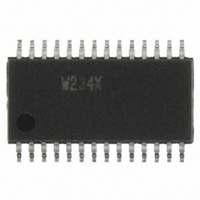
W234X Cypress Semiconductor Corp, W234X Datasheet - Page 8

W234X
Manufacturer Part Number
W234X
Description
CLOCK GEN DIR RAMBS DUAL 28TSSOP
Manufacturer
Cypress Semiconductor Corp
Type
Direct RAMbus Clock Generatorr
Datasheet
1.W234X.pdf
(14 pages)
Specifications of W234X
Input
CMOS
Output
CMOS
Frequency - Max
400MHz
Voltage - Supply
3.135 V ~ 3.465 V
Operating Temperature
0°C ~ 70°C
Mounting Type
Surface Mount
Package / Case
28-TSSOP
Frequency-max
400MHz
Lead Free Status / RoHS Status
Contains lead / RoHS non-compliant
Other names
428-1398
Available stocks
Company
Part Number
Manufacturer
Quantity
Price
Part Number:
W234X
Manufacturer:
ICW
Quantity:
20 000
Table 7. State Transition Latency Specifications
Figure 5 shows that the CLK Stop to Normal transition goes
through three phases. During t
specified and can have glitches. For t
clock output is enabled and must be glitch-free. For
t>t
Table 8. Distributed Loop Lock Time Specification
Document #: 38-07232 Rev. *B
t
CLKSETL
DISTLOCK
Transi-
Symbol
tion
B,D
G
M
A
C
K
H
E
E
N
F
L
J
, the clock output phase must be settled to within
Normal or Clk Stop
Min.
Power-Down
Power-Down
Power-Down
VDD ON
VDD ON
VDD ON
Clk Stop
Clk Stop
Normal
Normal
Normal
From
Test
Max.
5
CLKON
PWR_DWN
, the clock output is not
Clk Stop
Clk Stop
Clk Stop
Normal
Normal
Normal
Normal
Normal
Normal
CLKON
Unit
ms
Test
Test
Test
To
#
<t<t
Time from when CLK/CLK# output is settled to when the phase error between
SYNCLKN and PCLKM falls within the t
CLKSETL
t
t
t
t
t
t
t
POWERUP
POWERUP
POWERUP
POWERUP
POWERUP
POWERUP
t
POWERDN
Transition Latency
Symbol
t
CLKSETL
t
CLKOFF
t
CLKON
MULT
t
t
CTL
CTL
, the
50 ps of the phase before the clock output was disabled. At
this time, the clock output must also meet the voltage and tim-
ing specifications of Table 13. The outputs are in a high-imped-
ance state during the Clk Stop mode.
20 cycles Time from STOP# rising edge to CLK/CLK# out-
10 ns
Max.
3 ms
3 ms
3 ms
3 ms
3 ms
3 ms
1 ms
3 ms
3 ms
1 ms
5 ns
Time from PWR_DWN# to rising edge CLK/CLK#
output settled (excluding t
Time from PWR_DWN# rising edge until the in-
ternal PLL and clock has turned ON and settled.
Time from PWR_DWN# rising edge to CLK/CLK#
output settled (excluding t
Time from VDD is applied and settled until
CLK/CLK# output settled (excluding t
Time from VDD is applied and settled until
internal PLL and clock has turned ON and settled.
Time from VDD is applied and settled until
internal PLL and clock has turned ON and settled.
Time from when MULT0, MULT1, or MULT2
changed until CLK/CLK# output resettled (ex-
cluding t
Time from STOP# rising edge until CLK/CLK#
provides glitch-free clock edges.
put settled to within 50 ps of the phase before
CLK/CLK# was disabled.
Time from STOP# falling edge to CLK/CLK# out-
put disabled.
Time from when S0, S1, or S2 is changed until
CLK/CLK# output has resettled (excluding
t
Time from when S0, S1, or S2 is changed until
CLK/CLK# output has resettled (excluding
t
Time from PWR_DWN# falling edge to the device
in PWR_DWN#.
DISTLOCK
DISTLOCK
Description
DISTLOCK
ERR,PD
).
).
spec in Table 13.
).
Description
DISTLOCK
DISTLOCK
)
).
Page 8 of 14
DISTLOCK
W234
).


