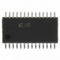
W234X Cypress Semiconductor Corp, W234X Datasheet - Page 5

W234X
Manufacturer Part Number
W234X
Description
CLOCK GEN DIR RAMBS DUAL 28TSSOP
Manufacturer
Cypress Semiconductor Corp
Type
Direct RAMbus Clock Generatorr
Datasheet
1.W234X.pdf
(14 pages)
Specifications of W234X
Input
CMOS
Output
CMOS
Frequency - Max
400MHz
Voltage - Supply
3.135 V ~ 3.465 V
Operating Temperature
0°C ~ 70°C
Mounting Type
Surface Mount
Package / Case
28-TSSOP
Frequency-max
400MHz
Lead Free Status / RoHS Status
Contains lead / RoHS non-compliant
Other names
428-1398
Available stocks
Company
Part Number
Manufacturer
Quantity
Price
Part Number:
W234X
Manufacturer:
ICW
Quantity:
20 000
Table 3. Bypass and Test Mode Selection
Table 4 shows the logic for selecting the Power-Down mode,
using the PWR_DWN# input signal. PWR_DWN# is active
LOW (enabled when 0). When PWR_DWN# is disabled, the
DRCG is in its normal mode. When PWR_DWN# is enabled,
the DRCG is put into a powered-off state, and the CLK and
CLK# outputs are three-stated.
Table 4. PWR_DWN# Mode Selection
Table of Frequencies and Gear Ratios
Table 5 shows several supported Pclk and Busclk frequencies,
the corresponding A and B dividers required in the DRCG PLL,
Table 5. Frequencies, Dividers, and Gear Ratios
Document #: 38-07232 Rev. *B
Normal
Bypass
Test
Vendor Test
A
Vendor Test
B
Reserved
Output Test
(OE)
Power-Down
Normal
Mode
Mode
Pclk
100
100
133
133
67
S0 S1 S2
PWR_DWN#
0
1
1
0
1
1
0
Refclk
0
0
1
0
0
1
1
33
50
50
67
67
1
0
0
0
0
1
1
1
X
By Pclk
PLLClk
RefClk
(int.)
Gnd
Busclk
-
-
-
-
PAClk
GND
CLK
267
300
400
267
400
PLLClk
RefClk
PAClk
CLK
Hi-Z
-
-
-
Synclk
PAClk#
CLK#
100
100
GND
67
75
67
PLLClk#
RefClk#
RefClk#
PAClk#
CLK#
-
-
-
A
8
6
8
4
6
and the corresponding M and N dividers in the gear ratio logic.
The column Ratio gives the Gear Ratio as defined Pclk/Synclk
(same as M and N). The column F@PD gives the divided down
frequency (in MHz) at the Phase Detector (
F@PD = PCLK/M = SYNCLK/N.
State Transitions
The clock source has three fundamental operating states.
Figure 4 shows the state diagram with each transition labelled
A through H. Note that the clock source output may NOT be
glitch-free during state transitions.
Upon powering up the device, the device can enter any state,
depending on the settings of the control signals, PWR_DWN#
and STOP#.
In Power-Down mode, the clock source is powered down with
the control signal, PWR_DWN#, equal to 0. The control sig-
nals S0, S1 and S2 must be stable before power is applied to
the device, and can only be changed in Power-Down mode
(PWR_DWN#=0). The reference inputs, VDDIR and VDDIPD,
may remain on or may be grounded during the Power-Down
mode.
The control signals MULT0, MULT1, and MULT2 can be used
in two ways. If they are changed during Power-Down mode,
then the Power-Down transition timings determine the settling
time of the DRCG. However, the MULT0, MULT1, and MULT2
control signals can also be changed during Normal mode.
When the MULT control signals are “hot swapped” in this man-
ner, the MULT transition timings determine the settling time of
the DRCG.
B
1
1
1
1
1
M
2
8
4
4
8
N
2
6
4
2
6
Ratio
1.33
1.33
1.0
1.0
2.0
Page 5 of 14
D
W234
F@PD
), where
12.5
16.7
33
25
33


