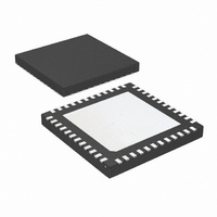
LMK01000ISQX/NOPB National Semiconductor, LMK01000ISQX/NOPB Datasheet - Page 13

LMK01000ISQX/NOPB
Manufacturer Part Number
LMK01000ISQX/NOPB
Description
IC CLK BUFFER/DVDR/DISTR 48-LLP
Manufacturer
National Semiconductor
Type
Fanout Buffer (Distribution), Dividerr
Datasheet
1.LMK01010ISQENOPB.pdf
(22 pages)
Specifications of LMK01000ISQX/NOPB
Number Of Circuits
1
Ratio - Input:output
2:8
Differential - Input:output
Yes/Yes
Input
Clock
Output
LVDS, LVPECL
Frequency - Max
1.6GHz
Voltage - Supply
3.15 V ~ 3.45 V
Operating Temperature
-40°C ~ 85°C
Mounting Type
Surface Mount
Package / Case
48-LLP
Frequency-max
1.6GHz
For Use With
LMK01000EVAL - BOARD EVALUATION FOR LMK01000
Lead Free Status / RoHS Status
Lead free / RoHS Compliant
Other names
LMK01000ISQX
Available stocks
Company
Part Number
Manufacturer
Quantity
Price
Company:
Part Number:
LMK01000ISQX/NOPB
Manufacturer:
IR
Quantity:
23 000
2.3.5 CLKoutX_EN bit -- Clock Output Enables
These bits control whether an individual clock output is en-
abled or not. If the EN_CLKout_Global bit is set to zero or if
GOE pin is held low, all CLKoutX_EN bit states will be ignored
and all clock outputs will be disabled.
2.4 REGISTER R9
R9 only needs to be programmed if Vboost is set to 1. Pro-
gram all other bits in R9 as indicated in register map (See
Section 2.2)
2.4.1 Vboost - Voltage Boost Bit
Enabling this bit sets all clock outputs in voltage boost mode
which increases the voltage at these outputs. This can im-
prove the noise floor performance of the output, but also
increases current consumption, and can cause the outputs to
be too high to meet the LVPECL/LVDS specifications.
CLKoutX_EN bit
Vboost
bit
0
1
0
1
Recommended to
hit voltage level
specifications for
LVPECL/LVDS
Voltage May
overdrive LVPECL/
LVDS
specifications, but
noise floor is about
2-4 dB better and
current
consumption is
increased
f
CLKoutX
MHz
GOE pin = High / No
EN_CLKout_Global
< 1300
Conditions
Connect 1
bit = 1
Insufficient voltage level for
LVDS/LVPECL
specifications, but saves
current
Voltage is
sufficient for
LVDS/
LEVPECL
specifications
. Current
consumption
is increased,
but noise floor
is about the
same.
1300 MHz
1500 MHz
f
CLKoutX
<
Disabled (default)
≤
CLKoutX State
Insufficient
voltage for
LVDS/
LVPECL
specifications
, but still
higher than
when
Vboost=0.
Increased
current
consumption.
1500 MHz
Enabled
1600 MHz
f
CLKoutX
≤
≤
13
2.5 REGISTER R14
The LMK01000 family requires register R14 to be pro-
grammed as shown in the register map (See Section 2.2).
2.5.1 POWERDOWN Bit -- Device Power Down
This bit can power down the device. Enabling this bit powers
down the entire device and all blocks, regardless of the state
of any of the other bits or pins.
2.5.2 EN_CLKout_Global Bit -- Global Clock Output
Enable
This bit overrides the individual CLKoutX_EN bits. When this
bit is set to 0, all clock outputs are disabled, regardless of the
state of any of the other bits or pins.
2.5.3 CLKin_SELECT Bit -- Device CLKin Select
This bit determines which CLKin pin is used.
EN_CLKout_Global bit
POWERDOWN bit
CLKin bit
0
1
0
1
0
1
Entire Device Powered Down
Normal Operation (default)
Normal Operation (default)
CLKin1 (default)
Clock Outputs
CLKin0
All Off
Mode
Mode
www.national.com


