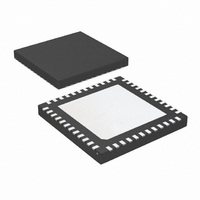
LMK01000ISQX/NOPB National Semiconductor, LMK01000ISQX/NOPB Datasheet - Page 7

LMK01000ISQX/NOPB
Manufacturer Part Number
LMK01000ISQX/NOPB
Description
IC CLK BUFFER/DVDR/DISTR 48-LLP
Manufacturer
National Semiconductor
Type
Fanout Buffer (Distribution), Dividerr
Datasheet
1.LMK01010ISQENOPB.pdf
(22 pages)
Specifications of LMK01000ISQX/NOPB
Number Of Circuits
1
Ratio - Input:output
2:8
Differential - Input:output
Yes/Yes
Input
Clock
Output
LVDS, LVPECL
Frequency - Max
1.6GHz
Voltage - Supply
3.15 V ~ 3.45 V
Operating Temperature
-40°C ~ 85°C
Mounting Type
Surface Mount
Package / Case
48-LLP
Frequency-max
1.6GHz
For Use With
LMK01000EVAL - BOARD EVALUATION FOR LMK01000
Lead Free Status / RoHS Status
Lead free / RoHS Compliant
Other names
LMK01000ISQX
Available stocks
Company
Part Number
Manufacturer
Quantity
Price
Company:
Part Number:
LMK01000ISQX/NOPB
Manufacturer:
IR
Quantity:
23 000
V
V
I
I
t
t
t
t
t
t
t
IH
IL
CS
CH
CWH
CWL
ES
CES
EWH
IH
IL
Note 4: The Electrical Characteristics tables list guaranteed specifications under the listed Recommended Operating Conditions except as otherwise modified
or specified by the Electrical Characteristics Conditions and/or Notes. Typical specifications are estimations only and are not guaranteed.
Note 5: See section 3.2 for more current consumption / power dissipation calculation information.
Note 6: For all frequencies the slew rate, SLEW
Note 7: The noise floor of the divider is measured as the far out phase noise of the divider. Typically this offset is 40 MHz, but for lower frequencies this
measurement offset can be as low as 5 MHz due to measurement equipment limitations. If the delay is used, then use section 1.3.
Note 8: Specification is guaranteed by characterization and is not tested in production.
Note 9: See characterization plots to see how this parameter varies over frequency.
Note 10: Applies to GOE, LD, and SYNC*.
Note 11: Applies to CLKuWire, DATAuWire, and LEuWire.
Serial Data Timing Diagram
Data bits set on the DATAuWire signal are clocked into a shift register, MSB first, on each rising edge of the CLKuWire signal. On
the rising edge of the LEuWire signal, the data is sent from the shift register to the addressed register determined by the LSB bits.
After the programming is complete the CLKuWire, DATAuWire, and LEuWire signals should be returned to a low state. The slew
rate of CLKuWire, DatauWire, and LEuWire should be at least 30 V/µs.
Symbol
High-Level Input Voltage
Low-Level Input Voltage
High-Level Input Current
Low-Level Input Current
Data to Clock Set Up Time
Data to Clock Hold Time
Clock Pulse Width High
Clock Pulse Width Low
Clock to Enable Set Up Time
Enable to Clock Set Up Time
Enable Pulse Width High
Parameter
CLKin1
Digital MICROWIRE Interfaces
, is measured between 20% and 80%.
V
V
See Data Input Timing
See Data Input Timing
See Data Input Timing
See Data Input Timing
See Data Input Timing
See Data Input Timing
See Data Input Timing
IH
IL
MICROWIRE Timing
= 0
= Vcc
7
Conditions
(Note
11)
Min
-5.0
-5.0
1.6
25
25
25
25
25
25
8
Typ
Max
Vcc
0.4
5.0
5.0
www.national.com
30042803
Units
µA
µA
ns
ns
ns
ns
ns
ns
ns
V
V


