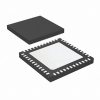
LMK01000ISQX/NOPB National Semiconductor, LMK01000ISQX/NOPB Datasheet - Page 18

LMK01000ISQX/NOPB
Manufacturer Part Number
LMK01000ISQX/NOPB
Description
IC CLK BUFFER/DVDR/DISTR 48-LLP
Manufacturer
National Semiconductor
Type
Fanout Buffer (Distribution), Dividerr
Datasheet
1.LMK01010ISQENOPB.pdf
(22 pages)
Specifications of LMK01000ISQX/NOPB
Number Of Circuits
1
Ratio - Input:output
2:8
Differential - Input:output
Yes/Yes
Input
Clock
Output
LVDS, LVPECL
Frequency - Max
1.6GHz
Voltage - Supply
3.15 V ~ 3.45 V
Operating Temperature
-40°C ~ 85°C
Mounting Type
Surface Mount
Package / Case
48-LLP
Frequency-max
1.6GHz
For Use With
LMK01000EVAL - BOARD EVALUATION FOR LMK01000
Lead Free Status / RoHS Status
Lead free / RoHS Compliant
Other names
LMK01000ISQX
Available stocks
Company
Part Number
Manufacturer
Quantity
Price
Company:
Part Number:
LMK01000ISQX/NOPB
Manufacturer:
IR
Quantity:
23 000
www.national.com
of the 120 Ω and 82 Ω resistors) is a valid termination as
shown in
When AC coupling an LVPECL driver use a 120 Ω emitter
resistor to provide a DC path to ground and ensure a 50 Ω
termination with the proper DC bias level for the receiver. The
typical DC bias voltage for LVPECL receivers is 2 V (See
Section 3.4.1). If the other driver is not used it should be ter-
minated with either a proper AC or DC termination. This latter
example of AC coupling a single-ended LVPECL signal can
be used to measure single-ended LVPECL performance us-
ing a spectrum analyzer or phase noise analyzer. When using
most RF test equipment no DC bias point (0 V DC) is expected
for safe and proper operation. The internal 50 Ω termination
the test equipment correctly terminates the LVPECL driver
being measured as shown in
LVPECL driver of a CLKoutX/CLKoutX* pair, be sure to prop-
erly terminated the unused driver.
FIGURE 10. Single-Ended LVPECL Operation, AC
FIGURE 8. Single-Ended LVPECL Operation, DC
FIGURE 9. Single-Ended LVPECL Operation, DC
Figure 9
Coupling, Thevenin Equivalent
for Vcc = 3.3 V.
Coupling
Coupling
Figure
10. When using only one
30042826
30042827
30042825
18
3.4.4 Conversion to LVCMOS Outputs
To drive an LVCMOS input with an LMK01000 family LVDS
or LVPECL output, an LVPECL/LVDS to LVCMOS converter
such
DS90LV028A, DS90LV048A, etc. is required. For best noise
performance, LVPECL provides a higher voltage swing into
input of the converter.
3.5 OSCin INPUT
In addition to LVDS and LVPECL inputs, OSCin can also be
driven with a sine wave. The OSCin input can be driven sin-
gle-ended or differentially with sine waves. These configura-
tions are shown in
Figure 13
operation for both differential and single-ended sources over
frequency. The part will operate at power levels below the
recommended power level, but as power decreases the PLL
noise performance will degrade. The VCO noise performance
will remain constant. At the recommended power level the
PLL phase noise degradation from full power operation (8
dBm) is less than 2 dB.
FIGURE 11. Single-Ended Sine Wave Input
as
FIGURE 12. Differential Sine Wave Input
shows the recommended power level for sine wave
National
Figure 11
Semiconductor's
and
Figure
12.
DS90LV018A,
30042829
30042828


