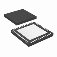
LMK01000ISQX/NOPB National Semiconductor, LMK01000ISQX/NOPB Datasheet - Page 9

LMK01000ISQX/NOPB
Manufacturer Part Number
LMK01000ISQX/NOPB
Description
IC CLK BUFFER/DVDR/DISTR 48-LLP
Manufacturer
National Semiconductor
Type
Fanout Buffer (Distribution), Dividerr
Datasheet
1.LMK01010ISQENOPB.pdf
(22 pages)
Specifications of LMK01000ISQX/NOPB
Number Of Circuits
1
Ratio - Input:output
2:8
Differential - Input:output
Yes/Yes
Input
Clock
Output
LVDS, LVPECL
Frequency - Max
1.6GHz
Voltage - Supply
3.15 V ~ 3.45 V
Operating Temperature
-40°C ~ 85°C
Mounting Type
Surface Mount
Package / Case
48-LLP
Frequency-max
1.6GHz
For Use With
LMK01000EVAL - BOARD EVALUATION FOR LMK01000
Lead Free Status / RoHS Status
Lead free / RoHS Compliant
Other names
LMK01000ISQX
Available stocks
Company
Part Number
Manufacturer
Quantity
Price
Company:
Part Number:
LMK01000ISQX/NOPB
Manufacturer:
IR
Quantity:
23 000
1.0 Functional Description
The LMK01000 family includes a programmable divider, a
phase synchronization circuit, a programmable delay, a clock
output mux, and an LVDS or LVPECL output buffer in each
channel. This allows multiple integer-related and phase-ad-
justed copies of the reference to be distributed to up to eight
system components.
This family of devices comes in a 48-pin LLP package that is
pin-to-pin and footprint compatible with other LMK02000/
LMK03000 family of clocking devices.
1.1 BIAS PIN
To properly use the device, bypass Bias (pin 36) with a low
leakage 1 µF capacitor connected to Vcc. This is important
for low noise performance.
1.2 CLKin0/CLKin0* and CLKin1/CLKin1 INPUT PORTS
The device can be driven either by the CLKin0/CLKin0* or the
CLKin1/CLKin1* pins. The choice of which one to use is soft-
ware selectable. These input ports must be AC coupled. To
drive these inputs in a single ended fashion, AC ground the
complementary input.
When choosing AC coupling capacitors for clock signals 0.1
µF is a good starting point, but lower frequencies may require
higher value capacitors while higher frequencies may use
lower value capacitors.
1.3 CLKout DELAYS
Each individual clock output includes a delay adjustment.
Clock output delay registers (CLKoutX_DLY) support a 150
ps step size and range from 0 to 2250 ps of total delay. When
the delay is enabled it adds to the output noise floor; the total
additive noise is 10(log( 10^(Output Noise Floor/10) + 10^
(Delay Noise Floor/10) ). Refer to the Typical Performance
Characteristics plots for the Delay Noise Floor information.
1.4 LVDS/LVPECL OUTPUTS
Each LVDS or LVPECL output may be disabled individually
by programming the CLKoutX_EN bits. All the outputs may
be disabled simultaneously by pulling the GOE pin low or
programming EN_CLKout_Global to 0.
1.5 GLOBAL CLOCK OUTPUT SYNCHRONIZATION
The SYNC* pin synchronizes the clock outputs. When the
SYNC* pin is held in a logic low state, the divided outputs are
also held in a logic low state. When the SYNC* pin goes high,
the divided clock outputs are activated and will transition to a
high state simultaneously. Clocks in the Bypassed state are
not affected by SYNC* and are always synchronized with the
divided outputs.
The SYNC* pin must be held low for greater than one clock
cycle of the Frequency Input port, also known as the distribu-
tion path. Once this low event has been registered, the out-
puts will not reflect the low state for four more cycles. When
the SYNC* pin becomes high, the outputs will not simultane-
ously transition high until four more distribution path clock
cycles have passed. See the SYNC* timing diagram for fur-
ther detail. In the timing diagram below the clocks are pro-
grammed as CLKout0_MUX = Bypassed, CLKout1_MUX =
Divided, CLKout1_DIV = 2, CLKout2_MUX = Divided, and
CLKout2_DIV = 4.
9
SYNC* Timing Diagram
The SYNC* pin provides an internal pull-up resistor as shown
on the functional block diagram. If the SYNC* pin is not ter-
minated externally the clock outputs will operate normally. If
the SYNC* function is not used, clock output synchronization
is not guaranteed.
1.6 CONNECTION TO LVDS OUTPUTS
LMK01000 and LMK01010 LVDS outputs can be connected
in AC or DC coupling configurations; however, in DC coupling
configuration, proper conditions must be presented by the
LVDS receiver. To ensure such conditions, we recommend
the usage of LVDS receivers without fail-safe or internal input
bias such as National Semiconductor's DS90LV110T. The
LMK01000 family LVDS drivers provide the adequate DC bias
for the LVDS receiver. We recommend AC coupling when
using LVDS receivers with fail-safe or internal input bias.
1.7 CLKout OUTPUT STATES
Each clock output may be individually enabled with the
CLKoutX_EN bits. Each individual output enable control bit is
gated with the Global Output Enable input pin (GOE) and the
Global Output Enable bit (EN_CLKout_Global).
All clock outputs can be disabled simultaneously if the GOE
pin is pulled low by an external signal or EN_CLKout_Global
is set to 0.
When an LVDS output is in the Off state, the outputs are at a
voltage of approximately 1.5 volts. When an LVPECL output
is in the Off state, the outputs are at a voltage of approximately
1 volt.
1.8 GLOBAL OUTPUT ENABLE
The GOE pin provides an internal pull-up resistor. If it is not
terminated externally, the clock output states are determined
by the Clock Output Enable bits (CLKoutX_EN) and the
EN_CLKout_Global bit.
1.9 POWER-ON-RESET
When supply voltage to the device increases monotonically
from ground to Vcc, the power-on-reset circuit sets all regis-
ters to their default values, which are specified in the General
Programming Information section. Voltage should be applied
to all Vcc pins simultaneously.
Don't care
CLKoutX
_EN bit
1
0
1
EN_CLKout
_Global bit
Don't care
1
0
1
Don't care
Don't care
High / No
GOE pin
Connect
Low
Output State
www.national.com
Clock X
Enabled
Low
Off
Off
30042804


