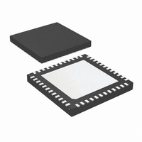
LMK01000ISQX/NOPB National Semiconductor, LMK01000ISQX/NOPB Datasheet - Page 3

LMK01000ISQX/NOPB
Manufacturer Part Number
LMK01000ISQX/NOPB
Description
IC CLK BUFFER/DVDR/DISTR 48-LLP
Manufacturer
National Semiconductor
Type
Fanout Buffer (Distribution), Dividerr
Datasheet
1.LMK01010ISQENOPB.pdf
(22 pages)
Specifications of LMK01000ISQX/NOPB
Number Of Circuits
1
Ratio - Input:output
2:8
Differential - Input:output
Yes/Yes
Input
Clock
Output
LVDS, LVPECL
Frequency - Max
1.6GHz
Voltage - Supply
3.15 V ~ 3.45 V
Operating Temperature
-40°C ~ 85°C
Mounting Type
Surface Mount
Package / Case
48-LLP
Frequency-max
1.6GHz
For Use With
LMK01000EVAL - BOARD EVALUATION FOR LMK01000
Lead Free Status / RoHS Status
Lead free / RoHS Compliant
Other names
LMK01000ISQX
Available stocks
Company
Part Number
Manufacturer
Quantity
Price
Company:
Part Number:
LMK01000ISQX/NOPB
Manufacturer:
IR
Quantity:
23 000
30, 31, 33, 37, 40, 43, 46
3, 8, 13, 16, 19, 22, 26,
Pin Descriptions
The LMK01000 family is footprint compatible with the LMK03000/02000 family of devices. All CLKout pins are pin-to-pin compatible,
and CLKin0 and CLKin1 are equivalent to OSCin and Fin, respectively.
Device Configuration Information
2, 7, 9,10, 32
14, 15
17, 18
20, 21
23, 24
28, 29
34, 35
38, 39
41, 42
44, 45
47, 48
Pin #
1, 25
DAP
11
12
27
36
4
5
6
CLKout0
CLKout1
CLKout2
CLKout3
CLKout4
CLKout5
CLKout6
CLKout7
Output
Vcc8, Vcc9, Vcc10, Vcc11, Vcc12, Vcc13, Vcc14
Vcc1, Vcc2, Vcc3, Vcc4, Vcc5, Vcc6, Vcc7,
CLKout0, CLKout0*
CLKout1, CLKout1*
CLKout2, CLKout2*
CLKout3, CLKout3*
CLKout4, CLKout4*
CLKout5, CLKout5*
CLKout6, CLKout6*
CLKout7, CLKout7*
CLKin1, CLKin1*
CLKin0,CLKin0*
DATAuWire
Pin Name
CLKuWire
LEuWire
SYNC*
LMK01000
GND
GOE
DAP
Test
Bias
LVPECL
LVPECL
LVPECL
LVPECL
LVPECL
NC
LVDS
LVDS
LVDS
3
I/O
O
O
O
O
O
O
O
O
O
-
-
-
-
I
I
I
I
I
I
I
I
Ground
No Connect. Pin is not connected to the die.
Power Supply
MICROWIRE Clock Input
MICROWIRE Data Input
MICROWIRE Latch Enable Input
Global Output Enable
This is an output pin used strictly for test purposes
and should be not connected for normal operation.
However, any load of an impedance of more than 1
kΩ is acceptable.
Clock Output 0
Clock Output 1
Clock Output 2
Clock Output 3
Global Clock Output Synchronization
CLKin 0 Input; Must be AC coupled
CLKin 1 Input; Must be AC coupled
Bias Bypass
Clock Output 4
Clock Output 5
Clock Output 6
Clock Output 7
Die Attach Pad should be connected to ground.
LMK01010
LVDS
LVDS
LVDS
LVDS
LVDS
LVDS
LVDS
LVDS
Description
LMK01020
LVPECL
LVPECL
LVPECL
LVPECL
LVPECL
LVPECL
LVPECL
LVPECL
www.national.com


