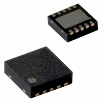
PCA8565BS/1,118 NXP Semiconductors, PCA8565BS/1,118 Datasheet - Page 29

PCA8565BS/1,118
Manufacturer Part Number
PCA8565BS/1,118
Description
IC CMOS RTC/CALENDAR 8-HVSON
Manufacturer
NXP Semiconductors
Type
Clock/Calendarr
Datasheet
1.PCA8565TS1118.pdf
(39 pages)
Specifications of PCA8565BS/1,118
Time Format
HH:MM:SS (24 hr)
Date Format
YY-MM-DD-dd
Interface
I²C, 2-Wire Serial
Voltage - Supply
1.8 V ~ 5.5 V
Operating Temperature
-40°C ~ 125°C
Mounting Type
Surface Mount
Package / Case
10-HVSON
Bus Type
Serial (2-Wire, I2C)
Operating Supply Voltage (typ)
2.5/3.3/5V
Operating Supply Voltage (max)
5.5V
Operating Supply Voltage (min)
1.8V
Operating Temperature (min)
-40C
Pin Count
10
Mounting
Surface Mount
Lead Free Status / RoHS Status
Lead free / RoHS Compliant
Memory Size
-
Lead Free Status / Rohs Status
Compliant
Other names
935282254118
PCA8565BS/1-T
PCA8565BS/1-T
PCA8565BS/1-T
PCA8565BS/1-T
Available stocks
Company
Part Number
Manufacturer
Quantity
Price
Company:
Part Number:
PCA8565BS/1,118
Manufacturer:
NXP
Quantity:
9 001
NXP Semiconductors
Table 31.
V
specified.
[1]
[2]
[3]
[4]
[5]
PCA8565_2
Product data sheet
Symbol
Oscillator
C
Quartz crystal parameters (f = 32.768 kHz)
R
C
C
CLKOUT output
I
f
t
t
t
t
t
t
t
t
t
t
t
C
2
SCL
HD;STA
SU;STA
LOW
HIGH
r
f
SU;DAT
HD;DAT
BUF
SU;STO
SP
DD
CLKOUT
f
C-bus timing characteristics
L(itg)
s
L
trim
b
osc
= 1.8 V to 5.5 V; V
Integrated load capacitance, C
For f
All timing values are valid within the operating supply voltage at ambient temperature and referenced to V
swing of V
A detailed description of the I
I
2
/f
C-bus access time between two STARTs or between a START and a STOP condition to this device must be less than one second.
osc
CLKOUT
Dynamic characteristics
SS
Parameter
integrated load capacitance
relative oscillator frequency variation
series resistance
load capacitance
trimmer capacitance
duty cycle on pin CLKOUT
SCL clock frequency
hold time (repeated) START condition
set-up time for a repeated START
condition
LOW period of the SCL clock
HIGH period of the SCL clock
rise time of both SDA and SCL signals
fall time of both SDA and SCL signals
data set-up time
data hold time
bus free time between a STOP and
START condition
set-up time for STOP condition
pulse width of spikes that must be
suppressed by the input filter
capacitive load for each bus line
= 1.024 kHz, 32 Hz and 1 Hz.
to V
12.2 Dynamic characteristics
DD
.
SS
= 0 V; T
2
C-bus specification is given in the document UM10204 .
L(itg)
amb
, is a calculation of C
= 40 C to +125 C; f
Rev. 02 — 16 June 2009
OSCI
Conditions
T
and C
amb
V
osc
DD
= 32.768 kHz; quartz R
= 25 C
OSCO
= 200 mV;
in series.
[3][4]
C
L itg
[1]
[2]
[5]
Min
15
-
-
-
5
-
-
0.6
0.6
1.3
0.6
-
-
100
0
4.7
0.6
-
-
=
s
--------------------------------------------
= 40 k ; C
C
C
OSCI
OSCI
Typ
25
2
-
10
-
50
-
-
-
-
-
-
-
-
-
-
-
-
-
+
Real time clock/calendar
C
C
IL
OSCO
L
OSCO
10
and V
= 8 pF; unless otherwise
-7
PCA8565
© NXP B.V. 2009. All rights reserved.
IH
with an input voltage
Max
35
-
40
-
25
-
400
-
-
-
-
0.3
0.3
-
-
-
-
50
400
29 of 39
Unit
pF
ppm
k
pF
pF
%
kHz
ns
ns
ns
pF
s
s
s
s
s
s
s
s


