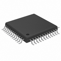
MAX1181ECM+D Maxim Integrated Products, MAX1181ECM+D Datasheet - Page 10

MAX1181ECM+D
Manufacturer Part Number
MAX1181ECM+D
Description
IC ADC 10BIT 80MSPS DUAL 48-TQFP
Manufacturer
Maxim Integrated Products
Datasheet
1.MAX1181ECMD.pdf
(20 pages)
Specifications of MAX1181ECM+D
Number Of Bits
10
Sampling Rate (per Second)
80M
Data Interface
Parallel
Number Of Converters
2
Power Dissipation (max)
291mW
Voltage Supply Source
Single Supply
Operating Temperature
-40°C ~ 85°C
Mounting Type
Surface Mount
Package / Case
48-TQFP Exposed Pad, 48-eTQFP, 48-HTQFP, 48-VQFP
Lead Free Status / RoHS Status
Lead free / RoHS Compliant
The MAX1181 uses a nine-stage, fully-differential
pipelined architecture (Figure 1), that allows for high-
speed conversion while minimizing power consump-
tion. Samples taken at the inputs move progressively
through the pipeline stages every half clock cycle.
Counting the delay through the output latch, the clock-
cycle latency is five clock cycles.
1.5-bit (two-comparator) flash ADCs convert the held-
input voltages into a digital code. The digital-to-analog
converters (DACs) convert the digitized results back
into analog voltages, which are then subtracted from
the original held-input signals. The resulting error sig-
nals are then multiplied by two, and the residues are
passed along to the next pipeline stages where the
process is repeated until the signals have been
processed by all nine stages. Digital error correction
compensates for ADC comparator offsets in each of
these pipeline stages and ensures no missing codes.
Figure 2 displays a simplified functional diagram of the
input track-and-hold (T/H) circuits in both track-and-
hold mode. In track mode, switches S1, S2a, S2b, S4a,
S4b, S5a and S5b are closed. The fully-differential cir-
cuits sample the input signals onto the two capacitors
(C2a and C2b) through switches S4a and S4b. S2a and
S2b set the common mode for the amplifier input, and
open simultaneously with S1, sampling the input wave-
form. Switches S4a and S4b are then opened before
switches S3a and S3b connect capacitors C1a and
C1b to the output of the amplifier and switch S4c is
closed. The resulting differential voltages are held on
Dual 10-Bit, 80Msps, 3V, Low-Power ADC
with Internal Reference and Parallel Outputs
10
______________________________________________________________________________________
PIN
40
41
42
43
44
45
46
47
48
—
Input Track-and-Hold (T/H) Circuits
REFOUT
NAME
REFIN
REFP
REFN
D5A
D6A
D7A
D8A
D9A
EP
Detailed Description
Three-State Digital Output, Bit 5, Channel A
Three-State Digital Output, Bit 6, Channel A
Three-State Digital Output, Bit 7, Channel A
Three-State Digital Output, Bit 8, Channel A
Three-State Digital Output, Bit 9 (MSB), Channel A
Internal Reference Voltage Output. May be connected to REFIN through a resistor or a resistor
divider.
Reference Input. V
Positive Reference Input/Output. Conversion range is ±(V
with a > 0.1µF capacitor.
Negative Reference Input/Output. Conversion range is ±(V
with a > 0.1µF capacitor.
Exposed Paddle. Connect to analog ground.
REFIN
= 2 x (V
REFP
capacitors C2a and C2b. The amplifiers are used to
charge capacitors C1a and C1b to the same values
originally held on C2a and C2b. These values are then
presented to the first-stage quantizers and isolate the
pipelines from the fast-changing inputs. The wide input
bandwidth T/H amplifiers allow the MAX1181 to track
and sample/hold analog inputs of high frequencies
(> Nyquist). Both ADC inputs (INA+, INB+, INA-, and
INB-) can be driven either differentially or single-ended.
Match the impedance of INA+ and INA-, as well as
INB+ and INB-, and set the common-mode voltage to
midsupply (V
The full-scale range of the MAX1181 is determined by
the internally generated voltage difference between
REFP (V
V
adjustable through the REFIN pin, which is provided for
this purpose.
REFOUT, REFP, COM (V
buffered low-impedance outputs.
The MAX1181 provides three modes of reference
operation:
In the internal reference mode, connect the internal ref-
erence output REFOUT to REFIN through a resistor
(e.g., 10kΩ) or resistor divider, if an application
requires a reduced full-scale range.
- V
REFIN
REFN
• Internal reference mode
• Buffered external reference mode
• Unbuffered external reference mode
FUNCTION
). Bypass to GND with a > 1nF capacitor.
/ 4). The full-scale range for both on-chip ADCs is
DD
Pin Description (continued)
DD
/ 2 + V
/ 2) for optimum performance.
REFP
Analog Inputs and Reference
REFP
REFIN
- V
- V
REFN
DD
REFN
/ 4) and REFN (V
/ 2) and REFN are internally
). Bypass to GND
). Bypass to GND
Configurations
DD
/ 2 -


