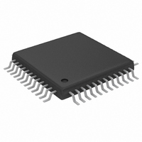
MAX1181ECM+D Maxim Integrated Products, MAX1181ECM+D Datasheet - Page 3

MAX1181ECM+D
Manufacturer Part Number
MAX1181ECM+D
Description
IC ADC 10BIT 80MSPS DUAL 48-TQFP
Manufacturer
Maxim Integrated Products
Datasheet
1.MAX1181ECMD.pdf
(20 pages)
Specifications of MAX1181ECM+D
Number Of Bits
10
Sampling Rate (per Second)
80M
Data Interface
Parallel
Number Of Converters
2
Power Dissipation (max)
291mW
Voltage Supply Source
Single Supply
Operating Temperature
-40°C ~ 85°C
Mounting Type
Surface Mount
Package / Case
48-TQFP Exposed Pad, 48-eTQFP, 48-HTQFP, 48-VQFP
Lead Free Status / RoHS Status
Lead free / RoHS Compliant
ELECTRICAL CHARACTERISTICS (continued)
(V
10kΩ resistor, V
T
Total Harmonic Distortion
(First Four Harmonics) (Note 3)
Intermodulation Distortion
(First Five Odd-Order IMDs)
Small-Signal Bandwidth
Full-Power Bandwidth
Aperture Delay
Aperture Jitter
Overdrive Recovery Time
Differential Gain
Differential Phase
Output Noise
INTERNAL REFERENCE
Reference Output Voltage
Reference Temperature
Coefficient
Load Regulation
BUFFERED EXTERNAL REFERENCE (V
REFIN Input Voltage
Positive Reference Output
Voltage
Negative Reference Output
Voltage
Differential Reference Output
Voltage Range
REFIN Resistance
Maximum REFP, COM Source
Current
Maximum REFP, COM Sink
Current
Maximum REFN Source Current
Maximum REFN Sink Current
UNBUFFERED EXTERNAL REFERENCE (V
REFP, REFN Input Resistance
MAX
DD
, unless otherwise noted. Typical values are at T
= 3V, OV
with Internal Reference and Parallel Outputs
PARAMETER
DD
IN
= 2.5V; 0.1µF and 1.0µF capacitors from REFP, REFN, and COM to GND; REFOUT connected to REFIN through a
= 2V
Dual 10-Bit, 80Msps, 3V, Low-Power ADC
_______________________________________________________________________________________
P-P
(differential with respect to COM), C
SYMBOL
I
I
REFOUT
SOURCE
SOURCE
V
R
TC
R
FPBW
V
V
ΔV
R
I
I
THD
IMD
REFIN
REFIN
SINK
SINK
REFP,
t
REFP
REFN
REFN
t
AD
AJ
REF
REF
REFIN
REFIN
f
f
f
f
f
(Note 4)
Input at -20dBFS, differential inputs
Input at -0.5dBFS, differential inputs
For 1.5 x full-scale input
INA+ = INA- = INB+ = INB- = COM
= 2.048V)
ΔV
Measured between REFP and COM and
REFN and COM
INA or B
INA or B
INA or B
INA or B
INA or B
REF
= AGND, reference voltage applied to REFP, REFN and COM )
A
= +25°C.) (Note 2)
= V
= 7.47MHz, T
= 20MHz, T
= 39.9MHz
= 38.1546MHz at -6.5dBFS
= 41.9532MHz at -6.5dBFS
REFP
L
- V
CONDITIONS
= 10pF at digital outputs (Note 1), f
REFN
A
A
= +25°C
= +25°C
0.95
MIN
CLK
= 83.333MHz, T
-73.5
±0.25
2.048
2.048
2.012
0.988
1.024
> 50
TYP
±3%
1.25
500
400
250
250
> 5
> 5
-73
-70
-70
0.2
±1
60
1
2
2
4
MAX
1.10
-64
-63
A
= T
degrees
LSB
ppm/°C
mV/mA
UNITS
ps
MHz
MHz
dBc
dBc
MΩ
mA
mA
kΩ
µA
µA
ns
ns
%
MIN
RMS
V
V
V
V
V
RMS
to
3


