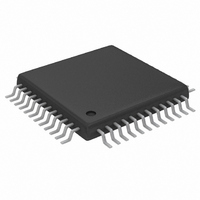
MAX1181ECM+D Maxim Integrated Products, MAX1181ECM+D Datasheet - Page 9

MAX1181ECM+D
Manufacturer Part Number
MAX1181ECM+D
Description
IC ADC 10BIT 80MSPS DUAL 48-TQFP
Manufacturer
Maxim Integrated Products
Datasheet
1.MAX1181ECMD.pdf
(20 pages)
Specifications of MAX1181ECM+D
Number Of Bits
10
Sampling Rate (per Second)
80M
Data Interface
Parallel
Number Of Converters
2
Power Dissipation (max)
291mW
Voltage Supply Source
Single Supply
Operating Temperature
-40°C ~ 85°C
Mounting Type
Surface Mount
Package / Case
48-TQFP Exposed Pad, 48-eTQFP, 48-HTQFP, 48-VQFP
Lead Free Status / RoHS Status
Lead free / RoHS Compliant
3, 7, 10, 13, 16
2, 6, 11, 14, 15
31, 34
32, 33
PIN
12
17
18
19
20
21
22
23
24
25
26
27
28
29
30
35
36
37
38
39
with Internal Reference and Parallel Outputs
1
4
5
8
9
Dual 10-Bit, 80Msps, 3V, Low-Power ADC
_______________________________________________________________________________________
NAME
SLEEP
OGND
OV
COM
INA+
INB+
GND
INA-
INB-
CLK
V
D9B
D8B
D7B
D6B
D5B
D4B
D3B
D2B
D1B
D0B
D0A
D1A
D2A
D3A
D4A
T/B
PD
OE
DD
DD
Common-Mode Voltage Input/Output. Bypass to GND with a ≥ 0.1µF capacitor.
Analog Supply Voltage. Bypass each supply pin to GND with a 0.1µF capacitor. The analog
supply voltage accepts a 2.7V to 3.6V input range.
Analog Ground
Channel ‘A’ Positive Analog Input. For single-ended operation, connect signal source to INA+.
Channel ‘A’ Negative Analog Input. For single-ended operation, connect INA- to COM.
Channel ‘B’ Negative Analog Input. For single-ended operation, connect INB- to COM.
Channel ‘B’ Positive Analog Input. For single-ended operation, connect signal source to INB+.
Converter Clock Input
T/B selects the ADC digital output format.
High: Two’s complement.
Low: Straight offset binary.
Sleep Mode Input.
High: Deactivates the two ADCs, but leaves the reference bias circuit active.
Low: Normal operation.
Power-Down Input.
High: Power-down mode.
Low: Normal operation.
Output Enable Input.
High: Digital outputs disabled.
Low: Digital outputs enabled.
Three-State Digital Output, Bit 9 (MSB), Channel B
Three-State Digital Output, Bit 8, Channel B
Three-State Digital Output, Bit 7, Channel B
Three-State Digital Output, Bit 6, Channel B
Three-State Digital Output, Bit 5, Channel B
Three-State Digital Output, Bit 4, Channel B
Three-State Digital Output, Bit 3, Channel B
Three-State Digital Output, Bit 2, Channel B
Three-State Digital Output, Bit 1, Channel B
Three-State Digital Output, Bit 0 (LSB), Channel B
Output Driver Ground
Output Driver Supply Voltage. Bypass each supply pin to OGND with a 0.1µF capacitor. The
digital supply voltage accepts a 1.7V to 3.6V input range.
Three-State Digital Output, Bit 0 (LSB), Channel A
Three-State Digital Output, Bit 1, Channel A
Three-State Digital Output, Bit 2, Channel A
Three-State Digital Output, Bit 3, Channel A
Three-State Digital Output, Bit 4, Channel A
FUNCTION
Pin Description
9


