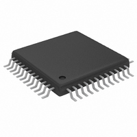
MAX1181ECM+D Maxim Integrated Products, MAX1181ECM+D Datasheet - Page 5

MAX1181ECM+D
Manufacturer Part Number
MAX1181ECM+D
Description
IC ADC 10BIT 80MSPS DUAL 48-TQFP
Manufacturer
Maxim Integrated Products
Datasheet
1.MAX1181ECMD.pdf
(20 pages)
Specifications of MAX1181ECM+D
Number Of Bits
10
Sampling Rate (per Second)
80M
Data Interface
Parallel
Number Of Converters
2
Power Dissipation (max)
291mW
Voltage Supply Source
Single Supply
Operating Temperature
-40°C ~ 85°C
Mounting Type
Surface Mount
Package / Case
48-TQFP Exposed Pad, 48-eTQFP, 48-HTQFP, 48-VQFP
Lead Free Status / RoHS Status
Lead free / RoHS Compliant
ELECTRICAL CHARACTERISTICS (continued)
(V
10kΩ resistor, V
T
Note 1: Equivalent dynamic performance is obtainable over full OV
Note 2: Specifications at ≥ +25°C are guaranteed by production test and < +25°C are guaranteed by design and characterization.
Note 3: SNR, SINAD, THD, SFDR, and HD3 are based on an analog input voltage of -0.5dBFS, referenced to a +1.024V full-scale
Note 4: Intermodulation distortion is the total power of the intermodulation products relative to the individual carrier. This number is
Note 5: Digital outputs settle to V
Note 6: With REFIN driven externally, REFP, COM, and REFN are left floating while powered down.
(V
wise noted.)
MAX
Power Supply Rejection
CLK Rise to Output Data Valid
Output Enable Time
Output Disable Time
CLK Pulse-Width High
CLK Pulse-Width Low
Wake-Up Time (Note 6)
CHANNEL-TO-CHANNEL MATCHING
Crosstalk
Gain Matching
Phase Matching
TIMING CHARACTERISTICS
DD
DD
-100
-10
-20
-30
-40
-50
-60
-70
-80
-90
0
, unless otherwise noted. Typical values are at T
= 3V, OV
= 3V, OV
0
FFT PLOT CHA (8192-POINT RECORD,
with Internal Reference and Parallel Outputs
CHA
input voltage range.
6dB or better, if referenced to the two-tone envelope.
PARAMETER
5
ANALOG INPUT FREQUENCY (MHz)
DIFFERENTIAL INPUT)
DD
DD
10
IN
= 2.5V; 0.1µF and 1.0µF capacitors from REFP, REFN, and COM to GND; REFOUT connected to REFIN through a
= 2.5V, internal reference, differential input at -0.5dBFS, f
= 2V
15
Dual 10-Bit, 80Msps, 3V, Low-Power ADC
_______________________________________________________________________________________
f
f
f
A
INA
INB
CLK
20
P-P
INA
= 6.0449MHz
= 7.5099MHz
= 80.0006MHz
= -0.46dBFS
(differential with respect to COM), C
25
30
IH
35
, V
SYMBOL
t
t
DISABLE
IL
ENABLE
t
PSRR
40
WAKE
. Parameter guaranteed by design.
t
t
t
DO
CH
CL
-100
-10
-20
-30
-40
-50
-60
-70
-80
-90
Offset
Gain
Figure 3 (Note 5)
Figure 4
Figure 4
Figure 3 clock period: 12ns
Figure 3 clock period: 12ns
Wakeup from sleep mode
Wakeup from shutdown
f
f
f
INA or B
INA or B
INA or B
0
0
FFT PLOT CHB (8192-POINT RECORD,
A
CHB
= +25°C.) (Note 2)
5
ANALOG INPUT FREQUENCY (MHz)
= 20MHz at -0.5dBFS
= 20MHz at -0.5dBFS
= 20MHz at -0.5dBFS
DIFFERENTIAL INPUT)
10
L
15
CONDITIONS
= 10pF at digital outputs (Note 1), f
f
f
f
A
DD
INA
INB
CLK
20
INB
= 6.0449MHz
= 7.5099MHz
= 80.0006MHz
range with reduced C
= -0.52dBFS
Typical Operating Characteristics
25
CLK
30
= 80.0006MHz, C
35
40
-100
L
-10
-20
-30
-40
-50
-60
-70
-80
-90
.
0
0
L
FFT PLOT CHA (8192-POINT RECORD,
CHA
MIN
≈ 10pF. T
CLK
5
ANALOG INPUT FREQUENCY (MHz)
DIFFERENTIAL INPUT)
10
= 83.333MHz, T
TYP
±0.2
±0.1
A
15
6 ±1
6 ±1
0.28
0.02
0.25
-70
1.5
1.5
10
= +25°C, unless other-
5
20
f
f
f
A
INA
INB
CLK
INA
25
MAX
±0.2
= 19.9123MHz
= 24.9123MHz
= 80.0006MHz
= -0.52dBFS
8
30
A
= T
degrees
UNITS
35
mV/V
MIN
%/V
dB
dB
ns
ns
ns
ns
ns
µs
40
to
5


