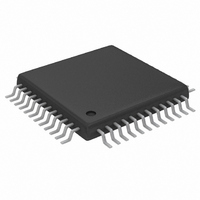
MAX1181ECM+D Maxim Integrated Products, MAX1181ECM+D Datasheet - Page 11

MAX1181ECM+D
Manufacturer Part Number
MAX1181ECM+D
Description
IC ADC 10BIT 80MSPS DUAL 48-TQFP
Manufacturer
Maxim Integrated Products
Datasheet
1.MAX1181ECMD.pdf
(20 pages)
Specifications of MAX1181ECM+D
Number Of Bits
10
Sampling Rate (per Second)
80M
Data Interface
Parallel
Number Of Converters
2
Power Dissipation (max)
291mW
Voltage Supply Source
Single Supply
Operating Temperature
-40°C ~ 85°C
Mounting Type
Surface Mount
Package / Case
48-TQFP Exposed Pad, 48-eTQFP, 48-HTQFP, 48-VQFP
Lead Free Status / RoHS Status
Lead free / RoHS Compliant
Figure 1. Pipelined Architecture––Stage Blocks
For stability and noise filtering purposes, bypass REFIN
with a > 10nF capacitor to GND. In internal reference
mode, REFOUT, COM, REFP, and REFN become low-
impedance outputs.
In the buffered external reference mode, adjust the ref-
erence voltage levels externally by applying a stable
and accurate voltage at REFIN. In this mode, COM,
REFP, and REFN become outputs. REFOUT may be left
open or connected to REFIN through a > 10kΩ resistor.
In the unbuffered external reference mode, connect
REFIN to GND. This deactivates the on-chip reference
buffers for REFP, COM, and REFN. With their buffers
shut down, these nodes become high impedance and
may be driven through separate external reference
sources.
The MAX1181’s CLK input accepts CMOS-compatible
clock signals. Since the interstage conversion of the
device depends on the repeatability of the rising and
falling edges of the external clock, use a clock with low
jitter and fast rise and fall times (< 2ns). In particular,
sampling occurs on the rising edge of the clock signal,
requiring this edge to provide lowest possible jitter. Any
significant aperture jitter would limit the SNR perfor-
mance of the on-chip ADCs as follows:
V
IN
with Internal Reference and Parallel Outputs
V
INA
T/H
FLASH
ADC
1.5 BITS
STAGE 1
T/H
Dual 10-Bit, 80Msps, 3V, Low-Power ADC
______________________________________________________________________________________
DAC
DIGITAL CORRECTION LOGIC
Σ
V
V
D9A–D0A
STAGE 2
INA
INB
= INPUT VOLTAGE BETWEEN INA+ AND INA- (DIFFERENTIAL OR SINGLE-ENDED)
= INPUT VOLTAGE BETWEEN INB+ AND INB- (DIFFERENTIAL OR SINGLE-ENDED)
10
x2
Clock Input (CLK)
V
OUT
STAGE 8
2-BIT FLASH
STAGE 9
ADC
V
IN
where f
t
Clock jitter is especially critical for undersampling
applications. The clock input should always be consid-
ered as an analog input and routed away from any ana-
log input or other digital signal lines.
The MAX1181 clock input operates with a voltage thresh-
old set to V
than 50% must meet the specifications for high and low
periods as stated in the Electrical Characteristics table.
Figure 3 depicts the relationship between the clock
input, analog input, and data output. The MAX1181
samples at the rising edge of the input clock. Output
data for channels A and B is valid on the next rising
edge of the input clock. The output data has an internal
latency of five clock cycles. Figure 4 also determines
the relationship between the input clock parameters
and the valid output data on channels A and B.
All digital outputs, D0A–D9A (Channel A) and D0B–D9B
(Channel B), are TTL/CMOS logic-compatible. There is a
AJ
V
is the time of the aperture jitter.
Digital Output Data, Output Data Format
INB
T/H
FLASH
ADC
IN
SNR = 20
1.5 BITS
Selection (T/B), Output Enable (
represents the analog input frequency and
STAGE 1
T/H
DD
/ 2. Clock inputs with a duty cycle other
DAC
System Timing Requirements
DIGITAL CORRECTION LOGIC
✕
log
Σ
D9B–D0B
STAGE 2
10
10
(1 / [2π x f
x2
V
OUT
STAGE 8
IN
✕
t
AJ
]),
2-BIT FLASH
STAGE 9
ADC
OE )
11


