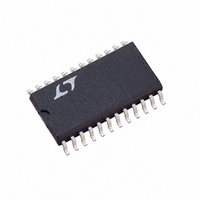
LTC1272-8CCSW#PBF Linear Technology, LTC1272-8CCSW#PBF Datasheet - Page 10

LTC1272-8CCSW#PBF
Manufacturer Part Number
LTC1272-8CCSW#PBF
Description
IC A/D CONV 12BIT SAMPLNG 24SOIC
Manufacturer
Linear Technology
Datasheet
1.LTC1272-3CCSW.pdf
(20 pages)
Specifications of LTC1272-8CCSW#PBF
Number Of Bits
12
Sampling Rate (per Second)
250k
Data Interface
Parallel
Number Of Converters
1
Power Dissipation (max)
75mW
Voltage Supply Source
Single Supply
Operating Temperature
0°C ~ 70°C
Mounting Type
Surface Mount
Package / Case
24-SOIC (0.300", 7.50mm Width)
Lead Free Status / RoHS Status
Lead free / RoHS Compliant
Available stocks
Company
Part Number
Manufacturer
Quantity
Price
A
LTC1272
Unipolar Operation
Figure 9 shows the ideal input/output characteristic for the
0V to 5V input range of the LTC1272. The code transitions
occur midway between successive integer LSB values
(i.e., 1/2LSB, 3/2LSBs, 5/2LSBs . . . FS – 3/2LSBs). The
output code is natural binary with 1 LSB = FS/4096 =
(5/4096)V = 1.22mV.
Unipolar Offset and Full-Scale Error Adjustment
In applications where absolute accuracy is important, then
offset and full-scale error can be adjusted to zero. Offset
10
PPLICATI
CURVATURE
CORRECTED
Figure 8. LTC1272 Internal 2.42V Reference
REFERENCE
BANDGAP
5V
O
U
S
CLK OUT
CS & RD
CLK IN
I FOR ATIO
BUSY
Figure 7. Operating Waveforms Using an External Clock Source for CLK IN
U
+
–
3
AGND
W
10 µF
0.1µF
2
LTC1272
V
REF
LTC1272 • TA10
TO DAC
U
(MSB)
DB11
50ns TYP
DB10
error must be adjusted before full-scale error. Figure 10
shows the extra components required for full-scale error
adjustment. Zero offset is achieved by adjusting the offset
of the op amp driving A
offset error apply 0.61mV (i.e., 1/2LBS) at V
the op amp offset voltage until the ADC output code
flickers between 0000 0000 0000 and 0000 0000 0001.
For zero full-scale error apply an analog input of 4.99817V
(i.e., FS – 3/2LSBs or last code transition) at V
R1 until the ADC output code flickers between 1111 1111
1110 and 1111 1111 1111.
Figure 9. LTC1272 Ideal Input/Output Transfer Characteristic
DB1
11...111
11...110
11...101
00...011
00...010
00...001
00...000
0
LSB
A
1
IN
(LSB)
DB0
, INPUT VOLTAGE (IN TERMS OF LSBs)
LSBs
2
IN
LSBs
FULL-SCALE
TRANSITION
3
(i.e., A1 in Figure 10). For zero
LTC1272 • TA08
FS = 5V
1LSB =
FS – 1LSB
LT1272 • TA11
––––
4096
FS
IN
FS
IN
and adjust
and adjust
1272fb
1272fb
1272fb


