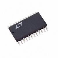
LTC1272-8CCSW#PBF Linear Technology, LTC1272-8CCSW#PBF Datasheet - Page 5

LTC1272-8CCSW#PBF
Manufacturer Part Number
LTC1272-8CCSW#PBF
Description
IC A/D CONV 12BIT SAMPLNG 24SOIC
Manufacturer
Linear Technology
Datasheet
1.LTC1272-3CCSW.pdf
(20 pages)
Specifications of LTC1272-8CCSW#PBF
Number Of Bits
12
Sampling Rate (per Second)
250k
Data Interface
Parallel
Number Of Converters
1
Power Dissipation (max)
75mW
Voltage Supply Source
Single Supply
Operating Temperature
0°C ~ 70°C
Mounting Type
Surface Mount
Package / Case
24-SOIC (0.300", 7.50mm Width)
Lead Free Status / RoHS Status
Lead free / RoHS Compliant
Available stocks
Company
Part Number
Manufacturer
Quantity
Price
A
V
an AD7572 socket, reverse the reference bypass capacitor
polarity and short the 10Ω series resistor.
AGND (Pin 3): Analog Ground.
D11 to D4 (Pins 4-11): Three-State Data Outputs.
DGND (Pin 12): Digital Ground.
D3/11 to D0/8 (Pins 13-16): Three-State Data Outputs.
CLK IN (Pin 17): Clock Input. An external TTL/CMOS
compatible clock may be applied to this pin or a crystal can
be connected between CLK IN and CLK OUT.
CLK OUT (Pin 18): Clock Output. An inverted CLK IN signal
appears at this pin.
Data Bus Output, CS and RD = LOW
*D11...D0/8 are the ADC data output pins.
TYPICAL PERFOR
PI
MNEMONIC*
HBEN = LOW
HBEN = HIGH
DB11...DB0 are the 12-bit conversion results, DB11 is the MSB.
IN
REF
U
(Pin 1): Analog Input, 0V to 5V Unipolar Input.
(Pin 2): 2.42V Reference Output. When plugging into
FU
U
C
TI
O
Pin 4
DB11
DB11
D11
U
S
W
DB10
DB10
Pin 5
D10
A
U
– 0.5
–1.0
1.0
0.5
CE
0
Pin 6
DB9
DB9
D9
0
0
Integral Nonlinearity
C
V
f
CLK
DD
512
HARA TERISTICS
= 5V
= 4MHz
Pin 7
DB8
DB8
D8
1024
1536
C
Pin 8
LOW
DB7
D7
CODE
2048
HBEN (Pin 19): High Byte Enable Input. This pin is used to
multiplex the internal 12-bit conversion result into the
lower bit outputs (D7 to D0/8). See table below. HBEN also
disables conversion starts when HIGH.
RD (Pin 20): Read Input. This active low signal starts a
conversion when CS and HBEN are low. RD also enables
the output drivers when CS is low.
CS (Pin 21): The Chip Select Input must be low for the ADC
to recognize RD and HBEN inputs.
BUSY (Pin 22): The BUSY Output is low when a conver-
sion is in progress.
NC (Pin 23): Not Connected Internally. The LTC1272 does
not require negative supply. This pin can accommodate
the –15V required by the AD7572 without problems.
V
Pin 9
LOW
DB6
DD
2560
D6
(Pin 24): Positive Supply, 5V.
3072
Pin 10
LOW
DB5
D5
LTC1272 • TPC01
3584
4096
Pin 11
LOW
DB4
D4
Pin 13
D3/11
DB11
DB3
Pin 14
D2/10
DB10
DB2
Pin 15
LTC1272
D1/9
DB1
DB9
Pin 16
D0/8
DB0
DB8
1272fb
5


