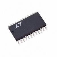
LTC1272-8CCSW#PBF Linear Technology, LTC1272-8CCSW#PBF Datasheet - Page 16

LTC1272-8CCSW#PBF
Manufacturer Part Number
LTC1272-8CCSW#PBF
Description
IC A/D CONV 12BIT SAMPLNG 24SOIC
Manufacturer
Linear Technology
Datasheet
1.LTC1272-3CCSW.pdf
(20 pages)
Specifications of LTC1272-8CCSW#PBF
Number Of Bits
12
Sampling Rate (per Second)
250k
Data Interface
Parallel
Number Of Converters
1
Power Dissipation (max)
75mW
Voltage Supply Source
Single Supply
Operating Temperature
0°C ~ 70°C
Mounting Type
Surface Mount
Package / Case
24-SOIC (0.300", 7.50mm Width)
Lead Free Status / RoHS Status
Lead free / RoHS Compliant
Available stocks
Company
Part Number
Manufacturer
Quantity
Price
A
At the beginning of the instruction cycle when the ADC
address is selected, BUSY and CS assert DTACK, so that
the MC68000 is forced into a Wait state. At the end of
conversion BUSY returns high and the conversion result
is placed in the D0 register of the microprocessor.
8085A, Z80 Microprocessor
Figure 19 shows a LTC1272 interface for the Z80 and
8085A. The LTC1272 is operating in the Slow Memory
Mode and a two byte read is required. Not shown in the
figure is the 8-bit latch required to demultiplex the 8085A
common address/data bus. A0 is used to assert HBEN, so
that an even address (HBEN = LOW) to the LTC1272 will
start a conversion and read the low data byte. An odd
address (HBEN = HIGH) will read the high data byte. This
LTC1272
16
PPLICATI
ADDITIONAL PINS OMITTED FOR CLARITY
LINEAR CIRCUITRY OMITTED FOR CLARITY
MC68000
8085A
Z80
DTACK
MREQ
Figure 19. LTC1272 8085A/Z80 Interface
WAIT
Figure 18. LTC1272 MC68000 Interface
R/W
D11
A23
A15
AS
D0
RD
A1
D7
D0
A0
O
U
S
ADDRESS BUS
EN
ADDRESS BUS
EN
DATA BUS
DATA BUS
I FOR ATIO
U
ADDRESS
ADDRESS
DECODE
DECODE
W
CS
BUSY
RD
D11
D0/8
CS
BUSY
RD
D7
D0/8
LTC1272
LTC1272
HBEN
LTC1272 • TA20
LTC1272 • TA21
A0
U
HBEN
is accomplished with the single 16-bit Load instruction
below.
This is a two byte read instruction which loads the ADC
data (address B000) into the HL register pair. During the
first read operation, BUSY forces the microprocessor to
Wait for the LTC1272 conversion. No Wait states are
inserted during the second read operation when the mi-
croprocessor is reading the high data byte.
TMS32010 Microcomputer
Figure 20 shows an LTC1272 TMS32010 interface. The
LTC1272 is operating in the ROM Mode. The interface is
designed for a maximum TMS32010 clock frequency of
18MHz but will typically work over the full TMS32010
clock frequency range.
The LTC1272 is mapped at a port address. The following
I/O instruction starts a conversion and reads the previous
conversion result into data memory.
When conversion is complete, a second I/O instruction
reads the up-to-date data into memory and starts another
conversion. A delay at least as long as the ADC conversion
time must be allowed between I/O instructions.
For the 8085A
For the Z80
LINEAR CIRCUITRY OMITTED FOR CLARITY
IN A,PA
TMS32010
Figure 20. LTC1272 TMS32010 Interface
DEN
PA2
PA0
D11
D0
PORT ADDRESS BUS
EN
LHLD (B000)
LDHL, (B000)
(PA = PORT ADDRESS)
DATA BUS
ADDRESS
DECODE
CS
RD
D11
D0/8
LTC1272
LTC1272 • TA22
HBEN
1272fb
1272fb
1272fb


