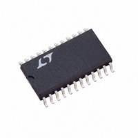
LTC1272-8CCSW#PBF Linear Technology, LTC1272-8CCSW#PBF Datasheet - Page 7

LTC1272-8CCSW#PBF
Manufacturer Part Number
LTC1272-8CCSW#PBF
Description
IC A/D CONV 12BIT SAMPLNG 24SOIC
Manufacturer
Linear Technology
Datasheet
1.LTC1272-3CCSW.pdf
(20 pages)
Specifications of LTC1272-8CCSW#PBF
Number Of Bits
12
Sampling Rate (per Second)
250k
Data Interface
Parallel
Number Of Converters
1
Power Dissipation (max)
75mW
Voltage Supply Source
Single Supply
Operating Temperature
0°C ~ 70°C
Mounting Type
Surface Mount
Package / Case
24-SOIC (0.300", 7.50mm Width)
Lead Free Status / RoHS Status
Lead free / RoHS Compliant
Available stocks
Company
Part Number
Manufacturer
Quantity
Price
A
Conversion Details
Conversion start is controlled by the CS, RD and HBEN
inputs. At the start of conversion the successive approxi-
mation register (SAR) is reset and the three-state data
outputs are enabled. Once a conversion cycle has begun
it cannot be restarted.
During conversion, the internal 12-bit capacitive DAC
output is sequenced by the SAR from the most significant
bit (MSB) to the least significant bit (LSB). Referring to
Figure 1, the A
capacitor through a 300Ω/2.7kΩ divider. The voltage
divider allows the LTC1272 to convert 0V to 5V input
signals while operating from a 4.5V supply. The conver-
sion has two phases: the sample phase and the convert
phase. During the sample phase, the comparator offset is
nulled by the feedback switch and the analog input is
stored as a charge on the sample-and-hold capacitor,
C
conversion until the next conversion is started. A mini-
mum delay between conversions (t
enough time for the analog input to be acquired. During the
convert phase, the comparator feedback switch opens,
putting the comparator into the compare mode. The
sample-and-hold capacitor is switched to ground inject-
ing the analog input charge onto the comparator summing
junction. This input charge is successively compared to
binary weighted charges supplied by the capacitive DAC.
Bit decisions are made by the comparator (zero crossing
detector) which checks the addition of each successive
weighted bit from the DAC output. The MSB decision is
made 50ns (typically) after the second falling edge of CLK
IN following a conversion start. Similarly, the succeeding
bit decisions are made approximately 50ns after a CLK IN
edge until the conversion is finished. At the end of a
conversion, the DAC output balances the A
The SAR contents (12-bit data word) which represent the
A
Sample-and-Hold and Dynamic Performance
Traditionally A/D converters have been characterized by
such specs as offset and full-scale errors, integral
SAMPLE
IN
PPLICATI
input signal are loaded into a 12-bit latch.
. This phase lasts from the end of the previous
IN
O
input connects to the sample-and-hold
U
S
I FOR ATIO
U
W
10
) of 1µs allows
IN
output charge.
U
nonlinearity and differential nonlinearity. These specs are
useful for characterizing an ADC’s DC or low frequency
signal performance.
These specs alone are not adequate to fully specify the
LTC1272 because of its high speed sampling ability. FFT
(Fast Fourrier Transform) test techniques are used to
characterize the LTC1272’s frequency response, distor-
tion and noise at the rated throughput.
By applying a low distortion sine wave and analyzing the
digital output using a FFT algorithm, the LTC1272’s spec-
tral content can be examined for frequencies outside the
fundamental. Figure 2 shows a typical LTC1272 FFT plot.
A
IN
300Ω
2.7k
Figure 2. LTC1272 Non-Averaged, 1024 Point FFT Plot.
f
S
= 250kHz, f
–100
–110
–40
–50
–60
–80
–90
–10
–20
–30
–70
SAMPLE
0
HOLD
0
20
IN
C
= 10kHz
SAMPLE
C
V
Figure 1. A
DAC
DAC
40
FREQUENCY (kHz)
60
DAC
IN
Input
80
SAMPLE
100
–
+
LTC1272 • TA23
COMPARATOR
SI
LTC1272
120
LTC1272 • TA07
LATCH
12-BIT
S
A
R
1272fb
7


