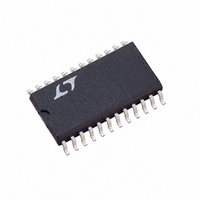
LTC1272-8CCSW#PBF Linear Technology, LTC1272-8CCSW#PBF Datasheet - Page 8

LTC1272-8CCSW#PBF
Manufacturer Part Number
LTC1272-8CCSW#PBF
Description
IC A/D CONV 12BIT SAMPLNG 24SOIC
Manufacturer
Linear Technology
Datasheet
1.LTC1272-3CCSW.pdf
(20 pages)
Specifications of LTC1272-8CCSW#PBF
Number Of Bits
12
Sampling Rate (per Second)
250k
Data Interface
Parallel
Number Of Converters
1
Power Dissipation (max)
75mW
Voltage Supply Source
Single Supply
Operating Temperature
0°C ~ 70°C
Mounting Type
Surface Mount
Package / Case
24-SOIC (0.300", 7.50mm Width)
Lead Free Status / RoHS Status
Lead free / RoHS Compliant
Available stocks
Company
Part Number
Manufacturer
Quantity
Price
A
Signal-to-Noise Ratio
The Signal-to-Noise Ratio (SNR) is the ratio between the
RMS amplitude of the fundamental input frequency to the
RMS amplitude of all other frequency components at the
A/D output. This includes distortion as well as noise
products and for this reason it is sometimes referred to as
Signal-to-Noise + Distortion [S/(N + D)]. The output is
band limited to frequencies from DC to one half the
sampling frequency. Figure 2 shows spectral content from
DC to 125kHz which is 1/2 the 250kHz sampling rate.
Effective Number of Bits
The effective number of bits (ENOBs) is a measurement of
the resolution of an A/D and is directly related to the
S/(N + D) by the equation:
where N is the effective number of bits of resolution and
S/(N + D) is expressed in dB. At the maximum sampling
rate of 250kHz the LTC1272 maintains 11.5 ENOBs or
better to 20kHz. Above 20kHz the ENOBs gradually de-
cline, as shown in Figure 3, due to increasing second
harmonic distortion. The noise floor remains approxi-
mately 90dB. The dynamic differential nonlinearity re-
mains good out to 120kHz as shown in Figure 4.
LTC1272
8
N = [S/(N + D) –1.76]/6.02,
Figure 3. LTC1272 Effective Number of Bits (ENOBs) vs Input
Frequency. f
PPLICATI
12
11
10
9
8
7
6
5
4
3
2
1
0
S
0
= 250kHz
f
V
S
DD
O
= 250kHz
20
= 5V
U
S
40
I FOR ATIO
f
IN
U
60
(kHz)
80
100
W
LT1272 • TPC07
120
U
Total Harmonic Distortion
Total Harmonic Distortion (THD) is the ratio of the RMS
sum of all harmonics of the input signal to the fundamental
itself. The harmonics are limited to the frequency band
between DC and one half the sampling frequency. THD is
expressed as: 20 LOG [
V
V
Nth harmonics.
Clock and Control Synchronization
For best analog performance, the LTC1272 clock should
be synchronized to the CS and RD control inputs as shown
in Figure 5, with at least 40ns separating convert start from
the nearest CLK IN edge. This ensures that transitions at
CLK IN and CLK OUT do not couple to the analog input and
get sampled by the sample-and-hold. The magnitude of
this feedthrough is only a few millivolts, but if CLK and
convert start (CS and RD) are asynchronous, frequency
components caused by mixing the clock and convert
signals may increase the apparent input noise.
When the clock and convert signals are synchronized,
small endpoint errors (offset and full-scale) are the most
that can be generated by clock feedthrough. Even these
errors (which can be trimmed out) can be eliminated by
ensuring that the start of a conversion (CS and RD’s falling
edge) does not occur within 40ns of a clock edge, as in
1
2
is the RMS amplitude of the fundamental frequency and
through V
Figure 4. LTC1272 Dynamic DNL. f
f
S
–0.5
–1.0
1.0
0.5
= 250kHz, f
0
0
0
N
are the amplitudes of the second through
IN
1
CODE (THOUSANDS)
= 122.25342kHz, V
√
V
2
2
2
+ V
3
2
+ ... + V
3
LTC1272 • TA24
CLK
CC
= 5V
= 4MHz,
N
4
2
/ V
1
] where
1272fb
1272fb
1272fb


