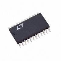
LTC1272-8CCSW#PBF Linear Technology, LTC1272-8CCSW#PBF Datasheet - Page 9

LTC1272-8CCSW#PBF
Manufacturer Part Number
LTC1272-8CCSW#PBF
Description
IC A/D CONV 12BIT SAMPLNG 24SOIC
Manufacturer
Linear Technology
Datasheet
1.LTC1272-3CCSW.pdf
(20 pages)
Specifications of LTC1272-8CCSW#PBF
Number Of Bits
12
Sampling Rate (per Second)
250k
Data Interface
Parallel
Number Of Converters
1
Power Dissipation (max)
75mW
Voltage Supply Source
Single Supply
Operating Temperature
0°C ~ 70°C
Mounting Type
Surface Mount
Package / Case
24-SOIC (0.300", 7.50mm Width)
Lead Free Status / RoHS Status
Lead free / RoHS Compliant
Available stocks
Company
Part Number
Manufacturer
Quantity
Price
Figure 5. Nevertheless, even without observing this guide-
line, the LTC1272 is still compatible with AD7572 synchro-
nization modes, with no increase in linearity error. This
means that either the falling or rising edge of CLK IN may
be near RD’s falling edge.
Driving the Analog Input
The analog input of the LTC1272 is much easier to drive
than that of the AD7572. The input current is not modu-
lated by the DAC as in the AD7572. It has only one small
current spike from charging the sample-and-hold capaci-
tor at the end of the conversion. During the conversion the
analog input draws only DC current. The only requirement
is that the amplifier driving the analog input must settle
after the small current spike before the next conversion is
started. Any op amp that settles in 1µs to small current
transients will allow maximum speed operation. If slower
op amps are used, more settling time can be provided by
increasing the time between conversions. Suitable de-
vices capable of driving the LTC1272 A
LT1006 and LT1007 op amps.
Internal Clock Oscillator
Figure 6 shows the LTC1272 internal clock circuit. A
crystal or ceramic resonator may be connected between
CLK IN (Pin 17) and CLK OUT (Pin 18) to provide a clock
oscillator for ADC timing. Alternatively the crystal/resona-
tor may be omitted and an external clock source may be
A
PPLICATI
O
U
S
CS & RD
CLK IN
I FOR ATIO
BUSY
U
*
UNCERTAIN CONVERSION TIME FOR 30ns < t
THE LTC1272 IS ALSO COMPATIBLE WITH THE AD7572 SYNCHRONIZATION MODES.
t
2
W
Figure 5. RD and CLK IN for Synchronous Operation
IN
t
14
≥ 40ns*
input include the
U
(MSB)
DB11
14
< 180ns
t
connected to CLK IN. For an external clock the duty cycle
is not critical. An inverted CLK IN signal will appear at the
CLK OUT pin as shown in the operating waveforms of
Figure 7. Capacitance on the CLK OUT pin should be
minimized for best analog performance.
Internal Reference
The LTC1272 has an on-chip, temperature compensated,
curvature corrected, bandgap reference, which is factory
trimmed to 2.42V ±1%. It is internally connected to the
DAC and is also available at pin 2 to provide up to 1mA
current to an external load.
For minimum code transition noise the reference output
should be decoupled with a capacitor to filter wideband
noise from the reference (10µF tantalum in parallel with a
0.1µF ceramic). A simplified schematic of the reference
with its recommended decoupling is shown in Figure 8.
CONV
DB10
NOTES:
LTC1272-3 – 4MHz CRYSTAL/CERAMIC RESONATOR
LTC1272-8 – 1.6MHz CRYSTAL/CERAMIC RESONATOR
C1
C2
Figure 6. LTC1272 Internal Clock Circuit
DB1
CLK OUT
CLK IN
18
17
(LSB)
DB0
LTC1272 • TA06
t
13
1M
LTC1272
LTC1272
LTC1272 • TA09
CLOCK
1272fb
9


