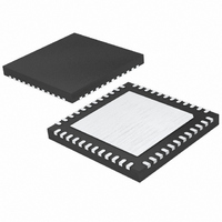
LTC2234IUK Linear Technology, LTC2234IUK Datasheet - Page 15

LTC2234IUK
Manufacturer Part Number
LTC2234IUK
Description
IC ADC 10BIT 135MSPS SAMPL 48QFN
Manufacturer
Linear Technology
Datasheet
1.LTC2234IUKPBF.pdf
(24 pages)
Specifications of LTC2234IUK
Number Of Bits
10
Sampling Rate (per Second)
135M
Data Interface
Parallel
Number Of Converters
1
Power Dissipation (max)
680mW
Voltage Supply Source
Single Supply
Operating Temperature
-40°C ~ 85°C
Mounting Type
Surface Mount
Package / Case
48-WFQFN, Exposed Pad
Lead Free Status / RoHS Status
Contains lead / RoHS non-compliant
Available stocks
Company
Part Number
Manufacturer
Quantity
Price
Company:
Part Number:
LTC2234IUK#PBF
Manufacturer:
Linear Technology
Quantity:
135
APPLICATIO S I FOR ATIO
signal at its optimum DC level. Terminating on the trans-
former secondary is desirable, as this provides a common
mode path for charging glitches caused by the sample and
hold. Figure 3 shows a 1:1 turns ratio transformer. Other
turns ratios can be used if the source impedance seen by
the ADC does not exceed 100Ω for each ADC input. A
disadvantage of using a transformer is the loss of low
frequency response. Most small RF transformers have
poor performance at frequencies below 1MHz.
Figure 4 demonstrates the use of a differential amplifier to
convert a single ended input signal into a differential input
signal. The advantage of this method is that it provides low
frequency input response; however, the limited gain band-
width of most op amps will limit the SFDR at high input
frequencies.
Figure 5 shows a single-ended input circuit. The imped-
ance seen by the analog inputs should be matched. This
circuit is not recommended if low distortion is required.
The 25Ω resistors and 12pF capacitor on the analog inputs
serve two purposes: isolating the drive circuitry from the
sample-and-hold charging glitches and limiting the
wideband noise at the converter input. For input frequen-
cies higher than 100MHz, the capacitor may need to be
decreased to prevent excessive signal loss.
ANALOG
AMPLIFIER = LTC6600-20,
"LT1993", ETC.
INPUT
Figure 4. Differential Drive with an Amplifier
DIFFERENTIAL
HIGH SPEED
AMPLIFIER
CM
+
–
U
–
+
25Ω
25Ω
3pF
U
3pF
2.2µF
12pF
W
V
A
A
CM
IN
IN
+
–
LTC2234
U
2234 F04
For input frequencies above 100MHz the input circuits of
Figure 6, 7 and 8 are recommended. The balun trans-
former gives better high frequency response than a flux
coupled center tapped transformer. The coupling capaci-
tors allow the analog inputs to be DC biased at 1.6V. In
Figure 8 the series inductors are impedance matching
elements that maximize the ADC bandwidth.
Reference Operation
Figure 9 shows the LTC2234 reference circuitry consisting
of a 1.6V bandgap reference, a difference amplifier and
switching and control circuit. The internal voltage refer-
ence can be configured for two pin selectable input ranges
of 2V (±1V differential) or 1V (±0.5V differential). Tying the
SENSE pin to V
pin to V
The 1.6V bandgap reference serves two functions: its
output provides a DC bias point for setting the common
mode voltage of any external input circuitry; additionally,
the reference is used with a difference amplifier to gener-
ate the differential reference levels needed by the internal
ADC circuitry. An external bypass capacitor is required for
the 1.6V reference output, V
frequency low impedance path to ground for internal and
external circuitry.
ANALOG
INPUT
CM
selects the 1V range.
0.1µF
DD
Figure 5. Single-Ended Drive
selects the 2V range; tying the SENSE
1k
1k
0.1µF
25Ω
25Ω
CM
. This provides a high
12pF
2.2µF
V
A
A
CM
IN
IN
LTC2234
+
–
LTC2234
2234 F05
15
2234fa


