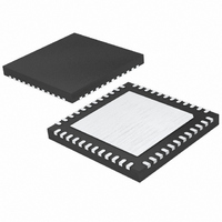
LTC2234IUK Linear Technology, LTC2234IUK Datasheet - Page 9

LTC2234IUK
Manufacturer Part Number
LTC2234IUK
Description
IC ADC 10BIT 135MSPS SAMPL 48QFN
Manufacturer
Linear Technology
Datasheet
1.LTC2234IUKPBF.pdf
(24 pages)
Specifications of LTC2234IUK
Number Of Bits
10
Sampling Rate (per Second)
135M
Data Interface
Parallel
Number Of Converters
1
Power Dissipation (max)
680mW
Voltage Supply Source
Single Supply
Operating Temperature
-40°C ~ 85°C
Mounting Type
Surface Mount
Package / Case
48-WFQFN, Exposed Pad
Lead Free Status / RoHS Status
Contains lead / RoHS non-compliant
Available stocks
Company
Part Number
Manufacturer
Quantity
Price
Company:
Part Number:
LTC2234IUK#PBF
Manufacturer:
Linear Technology
Quantity:
135
PI FU CTIO S
A
A
REFHA (Pins 3, 4): ADC High Reference. Bypass to Pins
5, 6 with 0.1µF ceramic chip capacitor, to Pins 9, 10 with
a 2.2µF ceramic capacitor and to ground with a 1µF
ceramic capacitor.
REFLB (Pins 5, 6): ADC Low Reference. Bypass to Pins 5,
6 with 0.1µF ceramic chip capacitor. Do not connect to
Pins 9, 10.
REFHB (Pins 7, 8): ADC High Reference. Bypass to Pins
9, 10 with 0.1µF ceramic chip capacitor. Do not connect to
Pins 3, 4.
REFLA (Pins 9, 10): ADC Low Reference. Bypass to Pins
7, 8 with 0.1µF ceramic chip capacitor, to Pins 3, 4 with a
2.2µF ceramic capacitor and to ground with a 1µF ceramic
capacitor.
V
GND with 0.1µF ceramic chip capacitors. Adjacent pins
can share a bypass capacitor.
GND (Pins 13, 15, 45, 48): ADC Power Ground.
ENC+ (Pin 16): Encode Input. The input is sampled on the
positive edge.
ENC– (Pin 17): Encode Complement Input. The input is
sampled on the negative edge. Bypass to ground with
0.1µF ceramic for single-ended ENCODE signal.
SHDN (Pin 18): Shutdown Mode Selection Pin. Connect-
ing SHDN to GND and OE to GND results in normal
operation with the outputs enabled. Connecting SHDN to
GND and OE to V
outputs at high impedance. Connecting SHDN to V
OE to GND results in nap mode with the outputs at high
impedance. Connecting SHDN to V
results in sleep mode with the outputs at high impedance.
IN
IN
DD
U
+ (Pin 1): Positive Differential Analog Input.
– (Pin 2): Negative Differential Analog Input.
(Pins 11, 12, 14, 46, 47): 3.3V Supply. Bypass to
U
DD
U
results in normal operation with the
DD
and OE to V
DD
and
DD
OE (Pin 19): Output Enable Pin. Refer to SHDN pin
function.
CLOCKOUT (Pin 20): Data Valid Output. Latch data on the
falling edge of CLOCKOUT.
NC (Pins 21, 24): Do not connect these pins.
D0 – D9 (Pins 25, 26, 29, 30, 31, 34, 35, 36, 39, 40):
Digital Outputs. D9 is the MSB.
OGND (Pins 22, 27, 32, 38): Output Driver Ground.
OV
Output Drivers. Bypass to ground with 0.1µF ceramic chip
capacitors.
OF (Pin 41): Over/Under Flow Output. High when an over
or under flow has occurred.
MODE (Pin 42): Output Format and Clock Duty Cycle
Stabilizer Selection Pin. Connecting MODE to 0V selects
offset binary output format and turns the clock duty cycle
stabilizer off. Connecting MODE to 1/3 V
binary output format and turns the clock duty cycle stabi-
lizer on. Connecting MODE to 2/3 V
ment output format and turns the clock duty cycle stabi-
lizer on. Connecting MODE to V
output format and turns the clock duty cycle stabilizer off.
SENSE (Pin 43): Reference Programming Pin. Connecting
SENSE to V
input range. V
input range. An external reference greater than 0.5V and
less than 1V applied to SENSE selects an input range of
±V
V
Bypass to ground with 2.2µF ceramic chip capacitor.
Exposed Pad (Pin 49): ADC Power Ground. The exposed
pad on the bottom of the package needs to be soldered to
ground.
CM
SENSE
DD
(Pin 44): 1.6V Output and Input Common Mode Bias.
(Pins 23, 28, 33, 37): Positive Supply for the
. ±1V is the largest valid input range.
CM
DD
selects the internal reference and a ±0.5V
selects the internal reference and a ±1V
DD
selects 2’s complement
DD
selects 2’s comple-
LTC2234
DD
selects offset
2234fa
9


