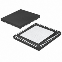
LTC2234IUK Linear Technology, LTC2234IUK Datasheet - Page 16

LTC2234IUK
Manufacturer Part Number
LTC2234IUK
Description
IC ADC 10BIT 135MSPS SAMPL 48QFN
Manufacturer
Linear Technology
Datasheet
1.LTC2234IUKPBF.pdf
(24 pages)
Specifications of LTC2234IUK
Number Of Bits
10
Sampling Rate (per Second)
135M
Data Interface
Parallel
Number Of Converters
1
Power Dissipation (max)
680mW
Voltage Supply Source
Single Supply
Operating Temperature
-40°C ~ 85°C
Mounting Type
Surface Mount
Package / Case
48-WFQFN, Exposed Pad
Lead Free Status / RoHS Status
Contains lead / RoHS non-compliant
Available stocks
Company
Part Number
Manufacturer
Quantity
Price
Company:
Part Number:
LTC2234IUK#PBF
Manufacturer:
Linear Technology
Quantity:
135
LTC2234
APPLICATIO S I FOR ATIO
16
The difference amplifier generates the high and low refer-
ence for the ADC. High speed switching circuits are
connected to these outputs and they must be externally
bypassed. Each output has four pins: two each of REFHA
and REFHB for the high reference and two each of REFLA
ANALOG
ANALOG
ANALOG
INPUT
INPUT
INPUT
Input Frequencies Between 100MHz and 250MHz
Input Frequencies Between 250MHz and 500MHz
Figure 6. Recommended Front End Circuit for
Figure 7. Recommended Front End Circuit for
Figure 8. Recommended Front End Circuit for
0.1µF
0.1µF
0.1µF
0.1µF
0.1µF
0.1µF
T1 = MA/COM ETC1-1-13
RESISTORS, CAPACITORS
ARE 0402 PACKAGE SIZE
T1 = MA/COM ETC1-1-13
RESISTORS, CAPACITORS
ARE 0402 PACKAGE SIZE
T1 = MA/COM ETC1-1-13
RESISTORS, CAPACITORS, INDUCTORS
ARE 0402 PACKAGE SIZE
Input Frequencies Above 500MHz
T1
T1
T1
U
25Ω
25Ω
25Ω
25Ω
25Ω
25Ω
U
0.1µF
0.1µF
0.1µF
4.7nH
12Ω
12Ω
4.7nH
W
2.2µF
8pF
2.2µF
2.2µF
2pF
V
V
V
A
A
A
A
A
A
CM
CM
CM
IN
IN
IN
IN
IN
IN
+
–
+
–
+
–
LTC2234
LTC2234
LTC2234
U
2234 F06
2234 F07
2234 F08
TIE TO V
TIE TO V
RANGE = 2 • V
and REFLB for the low reference. The multiple output pins
are needed to reduce package inductance. Bypass capaci-
tors must be connected as shown in Figure 9.
Other voltage ranges in between the pin selectable ranges
can be programmed with two external resistors as shown
in Figure 10. An external reference can be used by applying
its output directly or through a resistor divider to SENSE.
It is not recommended to drive the SENSE pin with a logic
device. The SENSE pin should be tied to the appropriate
level as close to the converter as possible. If the SENSE pin
is driven externally, it should be bypassed to ground as
close to the device as possible with a 1µF ceramic capacitor.
CM
0.5V < V
DD
FOR 2V RANGE;
FOR 1V RANGE;
SENSE
SENSE
1.6V
Figure 9. Equivalent Reference Circuit
1µF
1µF
< 1V
FOR
Figure 10. 1.6V Range ADC
2.2µF
12k
12k
1.6V
0.8V
0.1µF
2.2µF
0.1µF
SENSE
REFHA
REFHB
REFLB
REFLA
V
CM
SENSE
2.2µF
1µF
LTC2234
V
CONTROL
CM
DETECT
4Ω
RANGE
AND
LTC2234
1.6V BANDGAP
DIFF AMP
REFERENCE
2234 F10
INTERNAL ADC
HIGH REFERENCE
INTERNAL ADC
LOW REFERENCE
1V
BUFFER
0.5V
2234fa
2234 F09


